Storage and purge system for semiconductor wafers

Inactive Publication Date: 2009-02-26
SHMUELOV SHLOMO
View PDF22 Cites 44 Cited by
  • Summary
  • Abstract
  • Description
  • Claims
  • Application Information

AI Technical Summary

Benefits of technology

[0006]According to an embodiment of the the present invention there is provided a system for storage and maintenance of semiconductor wafers or reticles under fabrication between process steps of the fabrication. The system is configured as either a stocker, an overhead transport system (OHT) or an overhead buffer (OHB with gas-purge ports which mechanically mate with a standard receptacle of a wafer/reticle carrier. A control circuit is attached to the gas-purge ports which controls gas flow into the carrier through gas purge port said Control is performed even in the absence of a communications network attached to the control circuit. A local memory device is preferably attached to the control circuit. The local memory device stores a program accessed by the control circuit for the control of the gas flow. A communications network attached to the control circuit, transfers the program into the local memory device. The system preferably includes an input device for manually entering the program. and for manually entering commands (e.g STOP, START, NEW PROGRAM, PAUSE) to the control circuit. The gas purge ports and control circuit are preferably integrated with a previously existing storage system, a stocker, an overhead transport system (OHT) and/or overhead buffer/shelves (OHB). A reader, such as a bar code reader and/or radio fr

Problems solved by technology

However, since it is difficult and expensive to maintain a clean atmosphere of large volume, such as in a clean room, semiconductor substrate waf

Method used


Image

  • Storage and purge system for semiconductor wafers
  • Storage and purge system for semiconductor wafers
  • Storage and purge system for semiconductor wafers

Examples


Embodiment Construction

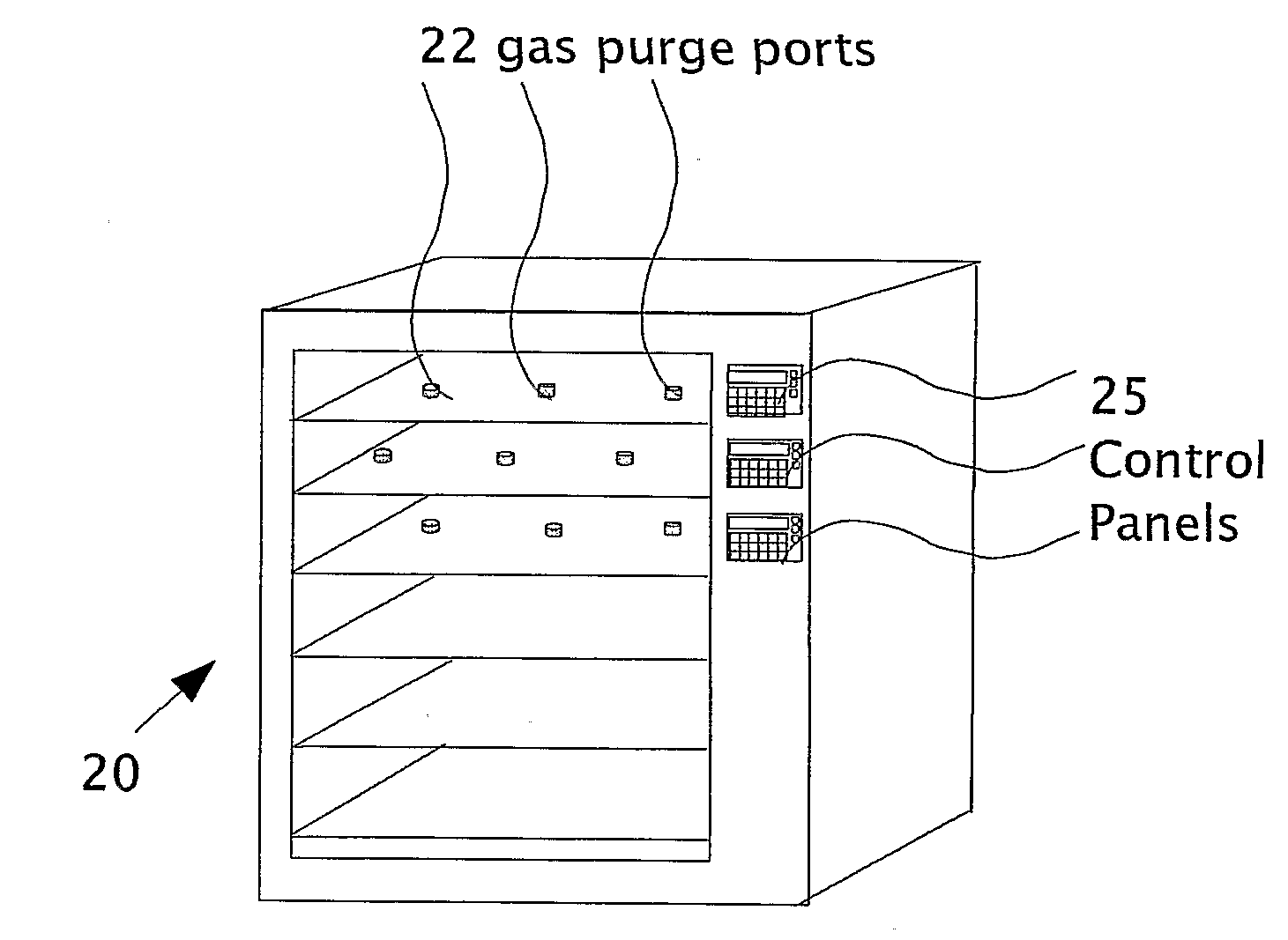
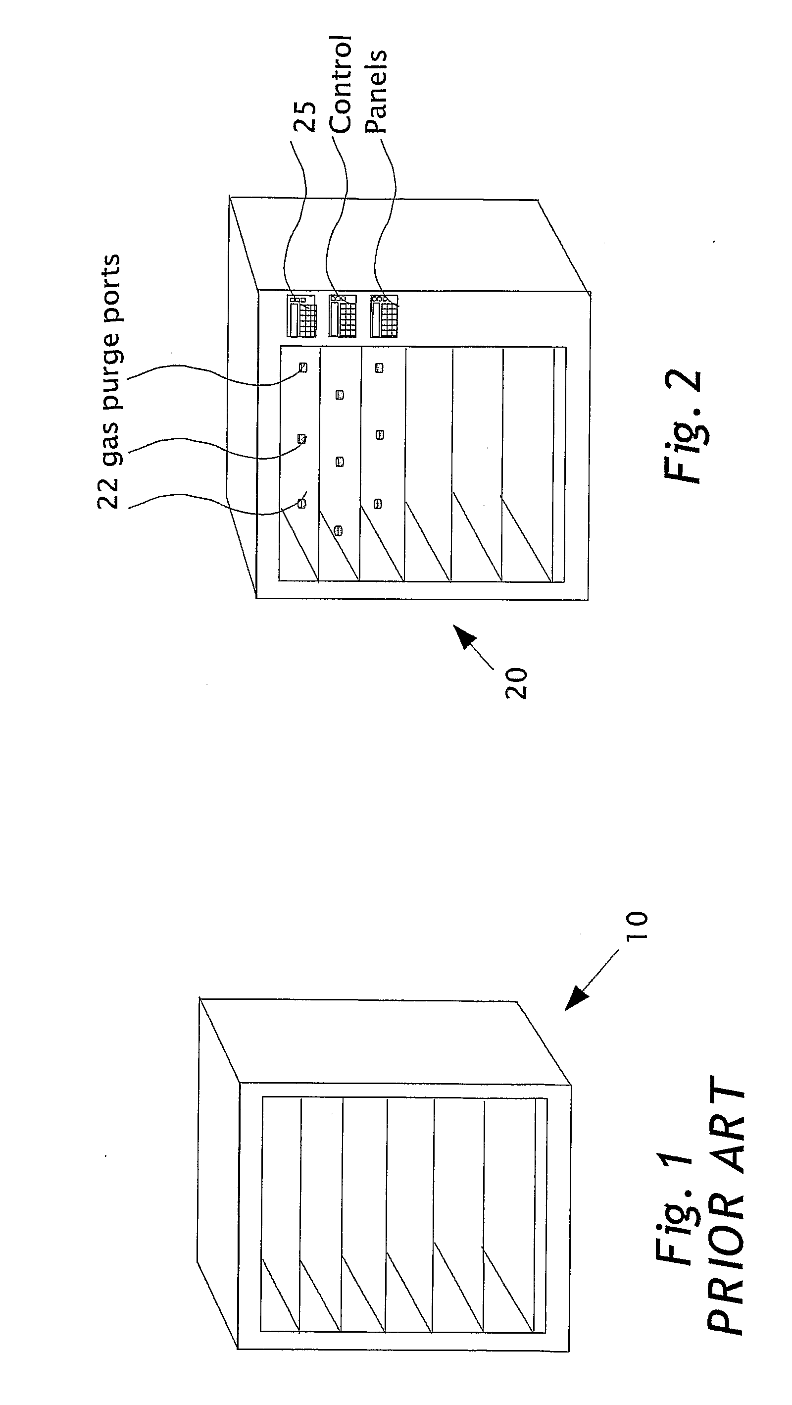
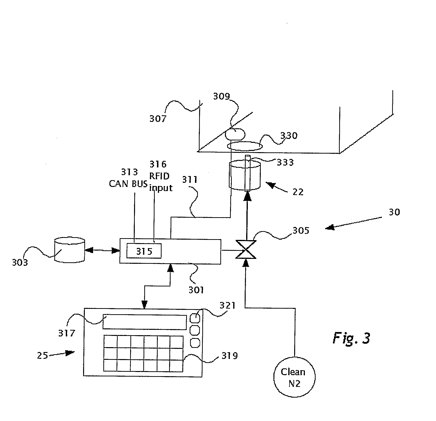
[0014]The present invention is a storage and purging system for semiconductor wafer carriers. The principles and operation of a storage and purging system for semiconductor wafer carriers according to the present invention, may be better understood with reference to the drawings and the accompanying description.

[0015]Before explaining embodiments of the invention in detail, it is to be understood that the invention is not limited in its application to the details of design and the arrangement of the components set forth in the following description or illustrated in the drawings. The invention is capable of other embodiments or of being practiced or carried out in various ways. Also, it is to be understood that the phraseology and terminology employed herein is for the purpose of description and should not be regarded as limiting.

[0016]By way of introduction, principal intentions of the present invention are to improve quality of integrated circuit manufacture by providing systemati...


PUM


Abstract

A system for storage and maintenance of semiconductor wafers or reticles under fabrication between process steps of the fabrication. The system is configured as either a stocker, an overhead transport system (OHT) or an overhead buffer (OHB with gas-purge ports which mechanically mate with a standard receptacle of a wafer/reticle carrier. A control circuit is attached to the gas-purge ports which controls gas flow into the carrier through gas purge port said Control is performed even in the absence of a communications network attached to the control circuit.

Description

FIELD AND BACKGROUND OF THE INVENTION[0001]The present invention relates to semiconductor fabrication in a clean room and particularly to a storage and purging system for semiconductor wafer carriers.[0002]Semiconductor integrated circuits are conventionally fabricated in clean rooms containing an atmosphere that is controlled to have a very low contamination content. The wafers are manufactured via chemical or other processes, and at times, are very sensitive to oxygen and humidity and other volatile contaminants. In order to avoid the potential damage to the material in process, the surrounding environment of the wafers and / or reticles is filled with a clean inert gas like nitrogen or clean dry air. In the past, the wafers / reticles were stored in gas cabinets which contained a clean environment. However, since it is difficult and expensive to maintain a clean atmosphere of large volume, such as in a clean room, semiconductor substrate wafers or masks are placed in mini-environment...

Claims


Application Information

Patent Timeline
IPC IPC(8): H01L21/67H01L21/677
CPCH01L21/67017H01L21/67294H01L21/67769H01L21/67393H01L21/67389
Inventor SHMUELOV, SHLOMO
Owner SHMUELOV SHLOMO
Why Eureka
Try Eureka