Electro-optical device and electronic apparatus

a technology of optical devices and electronic devices, applied in non-linear optics, instruments, optics, etc., can solve problems such as difficulty in narrowing the peripheral region, and achieve the effect of high-quality image display

Active Publication Date: 2009-04-09
138 EAST LCD ADVANCEMENTS LTD
View PDF4 Cites 15 Cited by
  • Summary
  • Abstract
  • Description
  • Claims
  • Application Information

AI Technical Summary

Benefits of technology

[0006]An advantage of some aspects of the invention is that it provides an electro-optical device, which is capable of realizing downsizing and performing a high-quality image display, and an electronic apparatus including the electro-optical device.
[0012]Accordingly, according to the electro-optical device of the invention, since the alignment mark is provided in the corner regions which are the so-called dead spaces, the region for providing only the alignment mark does not need to be ensured in the peripheral region and thus the peripheral region can narrow. For example, compared with the case where the alignment mark is provided in a region located inside the seal region, the pixel region surrounded by the seal region is increased or the region located inside the seal region in the peripheral region can narrow.
[0013]Accordingly, according to the liquid crystal device of the invention, the peripheral region of the liquid crystal device narrows with respect to the image display region and thus the liquid crystal device can be downsized without narrowing the image display region. That is, a high-quality image display can be performed and the liquid crystal device can be downsized. In particular, by this configuration, in a general manufacturing process of bonding a first mother substrate which becomes a plurality of first substrates and a second mother substrate which becomes a plurality of second substrates so as to form a plurality of liquid crystal devices and separately cutting the liquid crystal devices, more liquid crystal devices can be formed in the same area. In the case where several or several tens of liquid crystal devices are manufactured on the same mother substrate, for example, if the sizes of the first and second substrates are slightly reduced by several tenths mm or several mm, more liquid crystal devices can be formed on the same mother substrate by one column or a plurality of columns or one row or a plurality of rows. Accordingly, the significant effect can be obtained by slightly reducing the sizes of the first and second substrates.
[0014]As described above, according to the liquid crystal device of the invention, since the alignment marks are provided in the corner regions, it is possible to perform a high-quality image display and downsize the liquid crystal device.
[0022]According to this configuration, it is possible to arrange the alignment mark and the second conductive terminal on the first substrate with narrowing the peripheral region. Alternatively, it is possible to arrange the alignment mark and the first conductive terminal on the first substrate with increasing the pixel region.

Problems solved by technology

Thus, it is difficult to narrow the peripheral region.
In other words, the corner regions are the so-called dead spaces in which the seal material is not provided (that is, which does not become the seal region) since it is difficult to completely arrange the seal material along the outer edge of the second substrate when the seal material is provided so as to surround the pixel region.

Method used


Image

  • Electro-optical device and electronic apparatus
  • Electro-optical device and electronic apparatus
  • Electro-optical device and electronic apparatus

Examples


first embodiment

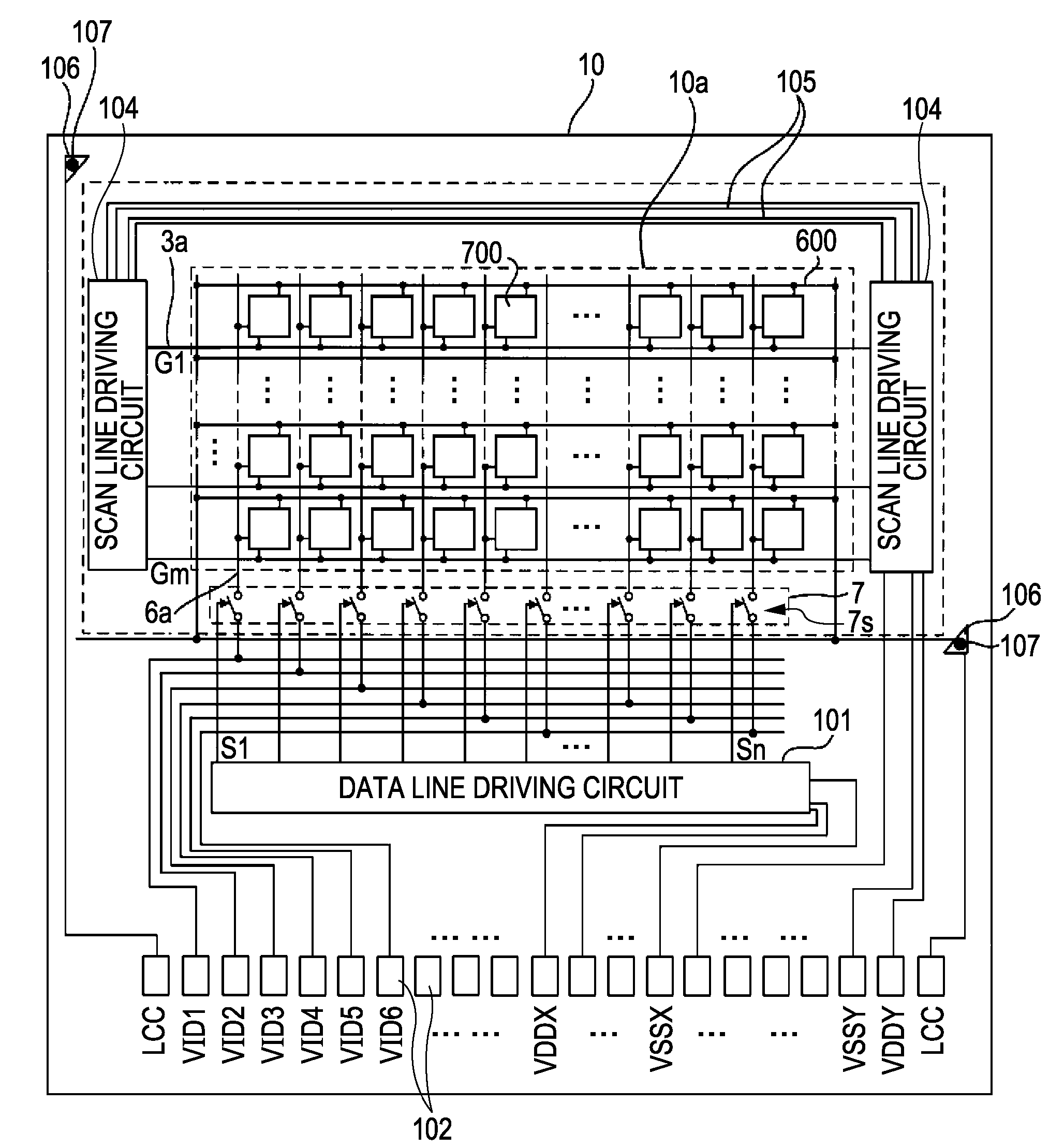
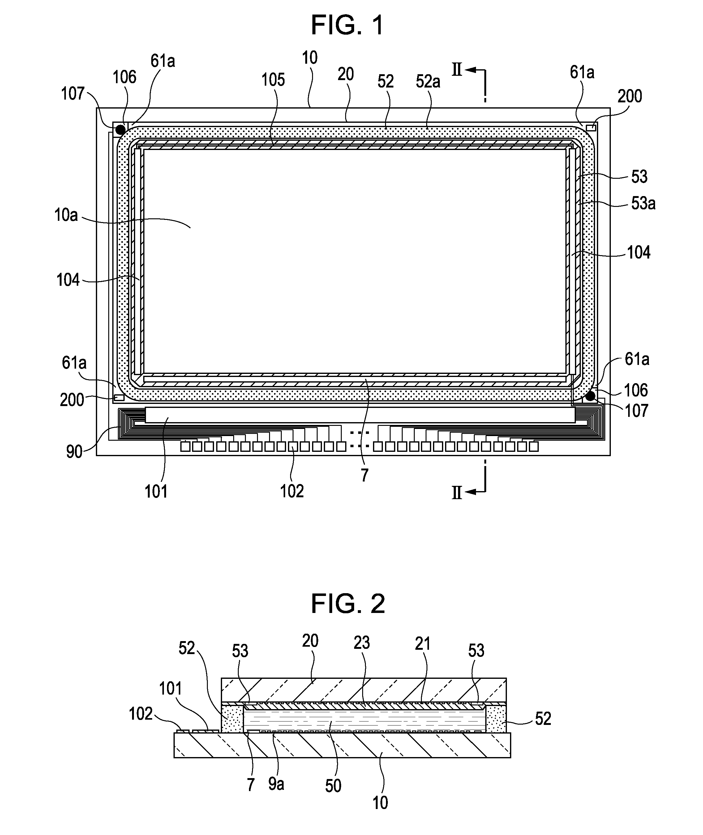
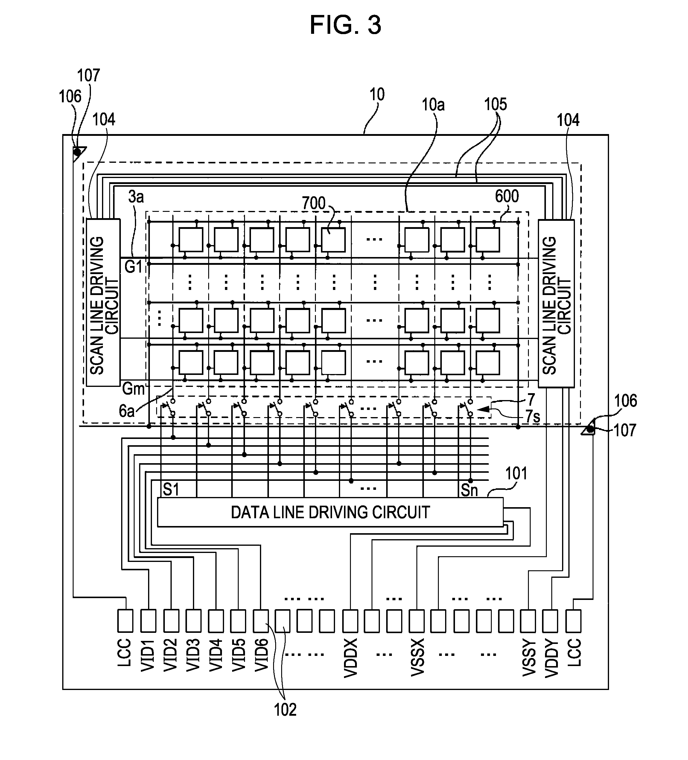
[0043]A liquid crystal device according to a first embodiment of the invention will be described with reference to FIGS. 1 to 7.

[0044]First, the overall configuration of the liquid crystal device according to the present embodiment will be described with reference to FIGS. 1 and 2. FIG. 1 is a plan view showing the overall configuration of a liquid crystal device according to a first embodiment of the invention. FIG. 2 is a cross-sectional view taken along line II-II of FIG. 1.

[0045]In FIGS. 1 and 2, the liquid crystal device according to the present embodiment includes a TFT array substrate 10 and a counter substrate 20 which face each other. Each of the TFT array substrate 10 and the counter substrate 20 has a rectangular shape. A liquid crystal layer 50 is sandwiched between the TFT array substrate 10 and the counter substrate 20, and the TFT array substrate 10 and the counter substrate 20 are bonded to each other by a seal material 52 provided in a seal region 52a located at the...

second embodiment

[0088]Next, a liquid crystal device according to a second embodiment will be described with reference to FIGS. 10 and 11. FIG. 10 is a plan view showing the whole configuration of the liquid crystal device according to the second embodiment. FIG. 11 is a view showing the positions of the alignment marks in the liquid crystal device according to the second embodiment. In FIGS. 10 and 11, the same components as the first embodiment shown in FIGS. 1 to 7 are denoted by the same reference numerals and the description thereof will be properly omitted.

[0089]In FIG. 10, the liquid crystal device according to the second embodiment is different from the liquid crystal device according to the first embodiment in that upper / lower conductive terminals 106b and alignment marks 200b are included instead of the upper / lower conductive terminals 106 and the alignment marks 200 of the first embodiment and is similar to the liquid crystal device according to the first embodiment in other points. The u...


PUM

PropertyMeasurementUnit
conductiveaaaaaaaaaa
sizeaaaaaaaaaa
sizesaaaaaaaaaa

Abstract

An electro-optical device includes a pair of first and second substrates. A pixel region on the first substrate. A seal material arranged along the periphery of the pixel region. An alignment mark located between the outer edge side of the second substrate and the seal material, The alignment mark is provided in at least one of four corner regions partially defined by four corners of the second substrate, and is used during alignment of the first and second substrates.

Description

BACKGROUND[0001]1. Technical Field[0002]The present invention relates to an electro-optical device such as a liquid crystal device and an electronic apparatus including the electro-optical device, such as a liquid crystal projector.[0003]2. Related Art[0004]As disclosed in JP-A-2005-181514, WO98 / 16867 and JP-A-2004-151343, an electro-optical device includes a pair of substrates bonded to each other by a seal material and an electro-optical material such as liquid crystal sandwiched between the substrates. Here, the seal material is arranged in a seal region along the periphery of a pixel region (or a pixel array region) in which a plurality of pixels are arranged. An alignment mark for aligning the pair of substrates at the time of the manufacture of the electro-optical device is provided in a predetermined region located on the inside (the pixel region side when viewed from the seal region) of the seal region of the substrates (see JP-A-2004-151343).[0005]In order to downsize such ...

Claims


Application Information

Patent Timeline
Patent Type & Authority Applications(United States)
IPC IPC(8): G02F1/1333
CPCG02F2001/133354G02F1/1339G02F1/133354
Inventor KONDO, MASAHIKO
Owner 138 EAST LCD ADVANCEMENTS LTD
Why Eureka
Try Eureka