Embedded DRAM Integrated Circuits With Extremely Thin Silicon-On-Insulator Pass Transistors

a technology of integrated circuits and transistors, applied in the direction of transistors, semiconductor devices, electrical devices, etc., can solve the problems of inherently vulnerable to variability, compromising memory cell functionality, and wreaking the effect of worsening tradeoffs

Active Publication Date: 2009-04-30
GLOBALFOUNDRIES US INC
View PDF11 Cites 46 Cited by
  • Summary
  • Abstract
  • Description
  • Claims
  • Application Information

AI Technical Summary

Problems solved by technology

The use of eDRAM as microprocessor cache, however, involves making tradeoffs between performance parameters, such as speed, retention time and power consumption, and production parameters, such as yield and design complexity.
Due to their small sizes, memory cells are especially susceptible to process-induced variations, which worsen these tradeoffs and compromise memory cell functionality.
Typically, an eDRAM cell calls for a bulk-silicon pass transistor with a heavily doped channel which, in addition to being sensitive to process non-uniformities, is inherently vulnerable to variability from random dopant fluctuations.
While solutions for addressing variability problems in microprocessor memories exist to better control device characteristics (e.g., better process control during manufacturing and careful cell layout), random dopant fluctuations present a fundamental limitation to improving eDRAM performance.
However, the integration of FinFETs with planar logic is difficult due to vertical topography, especially since DRAM processes generally rely on bulk silicon wafer substrates.
In addition, an entirely FinFET-based technology (both memory and logic) has yet to be implemented in the industry.
Thus, the use of FinFETs for eDRAM is not yet practical.

Method used


Image

  • Embedded DRAM Integrated Circuits With Extremely Thin Silicon-On-Insulator Pass Transistors
  • Embedded DRAM Integrated Circuits With Extremely Thin Silicon-On-Insulator Pass Transistors
  • Embedded DRAM Integrated Circuits With Extremely Thin Silicon-On-Insulator Pass Transistors

Examples


Embodiment Construction

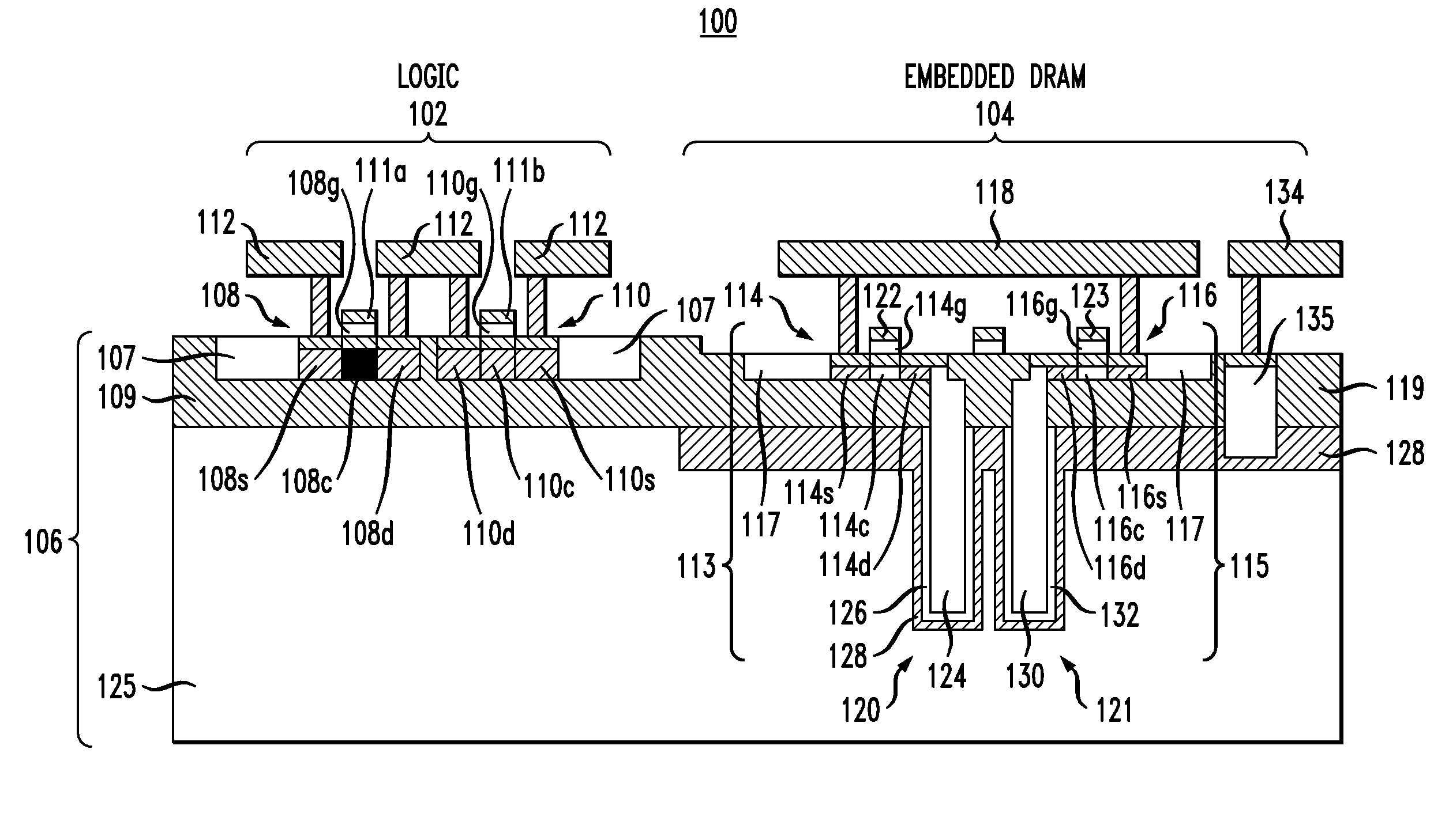
[0016]FIG. 1 is a cross-sectional diagram illustrating exemplary integrated circuit 100 having both a logic region 102 and an embedded dynamic random access memory (eDRAM) region 104. Namely, logic region 102 comprises logic transistors 108 and 110, and eDRAM region 104 comprises eDRAM cells 113 and 115 (having pass transistors 114 and 116, and trench capacitors 120 and 121, respectively), wherein the logic transistors and eDRAM cells are integrated on a common substrate 106.

[0017]Substrate 106 comprises a silicon-on-insulator (SOI) substrate having at least two distinct regions therein, one region corresponding to logic region 102 and one region corresponding to eDRAM region 104. The region of substrate 106 corresponding to logic region 102 comprises a partially depleted SOI (PDSOI) region having a silicon (Si) layer 107 over a buried oxide (BOX) layer 109, wherein Si layer 107 has a thickness of between about 30 nanometers (nm) and about 100 nm and forms source, drain and channel ...


PUM


Abstract

Integrated circuits having combined memory and logic functions are provided. In one aspect, an integrated circuit is provided. The integrated circuit comprises: a substrate comprising a silicon layer over a BOX layer, wherein a select region of the silicon layer has a thickness of between about three nanometers and about 20 nanometers; at least one eDRAM cell comprising: at least one pass transistor having a pass transistor source region, a pass transistor drain region and a pass transistor channel region formed in the select region of the silicon layer; and a capacitor electrically connected to the pass transistor.

Description

FIELD OF THE INVENTION[0001]The present invention relates to integrated circuits with embedded dynamic random access memory (eDRAM), and more particularly, to techniques for improving eDRAM performance.BACKGROUND OF THE INVENTION[0002]It is a common practice to integrated memory and logic functions on a common semiconductor substrate. In such a configuration, when the memory function is performed by a dynamic random access memory (DRAM) cell, the circuitry is referred to as embedded DRAM (eDRAM).[0003]The use of eDRAM as microprocessor cache, however, involves making tradeoffs between performance parameters, such as speed, retention time and power consumption, and production parameters, such as yield and design complexity. Due to their small sizes, memory cells are especially susceptible to process-induced variations, which worsen these tradeoffs and compromise memory cell functionality. Thus, steps need to be taken to minimize process-induced variations.[0004]For example, reducing ...

Claims


Application Information

Patent Timeline
Patent Type & Authority Applications(United States)
IPC IPC(8): H01L21/84H01L27/12
CPCH01L21/84H01L27/1203H01L27/10894H10B12/09
Inventor CAI, JINCHANG, JOSEPHINECHANG, LELANDJI, BRIAN L.KOESTER, STEVEN JOHNMAJUMDAR, AMLAN
Owner GLOBALFOUNDRIES US INC
Why Eureka
Try Eureka