Antifuse element in which more than two values of information can be written

a technology of information and antifuse elements, applied in the field of antifuse elements, can solve the problems of low throughput and the inability to use laser trimmer equipment after packaging

Inactive Publication Date: 2009-05-07
ELPIDA MEMORY INC
View PDF2 Cites 37 Cited by
  • Summary
  • Abstract
  • Description
  • Claims
  • Application Information

AI Technical Summary

Problems solved by technology

However, such a circuit saving by the fuse includes such a fault that the throughput is low, and the laser trimmer apparatus can not be used after packaging.

Method used


Image

  • Antifuse element in which more than two values of information can be written
  • Antifuse element in which more than two values of information can be written
  • Antifuse element in which more than two values of information can be written

Examples


first exemplary embodiment

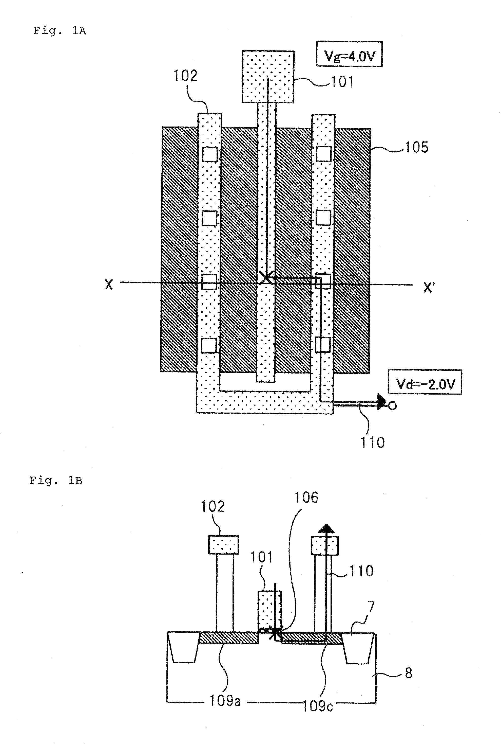
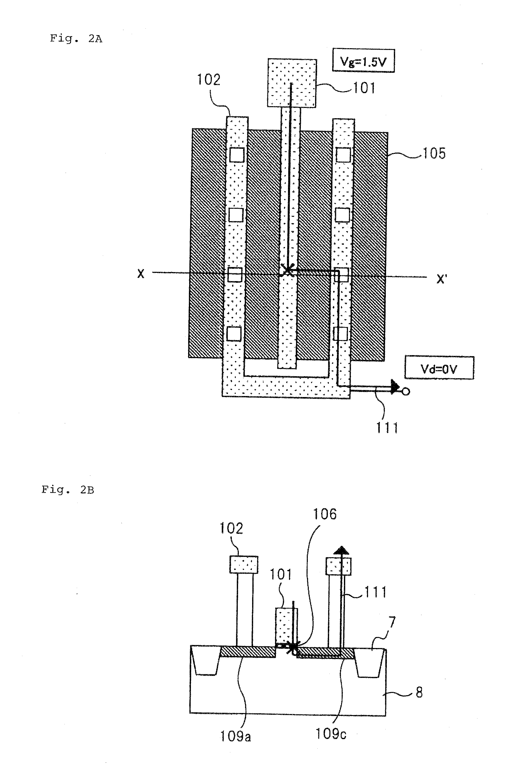
[0028]A configuration of an antifuse of the present exemplary embodiment will be described. The present exemplary embodiment will be described in such a case in which a maximum of five values of information can be recorded in a fuse.

[0029]FIG. 3A and FIG. 3B are views illustrating an exemplary configuration of the antifuse of the present exemplary embodiment. FIG. 3A is a plain view of the antifuse, and FIG. 3B is a cross-section view at line X-X′ of FIG. 3A.

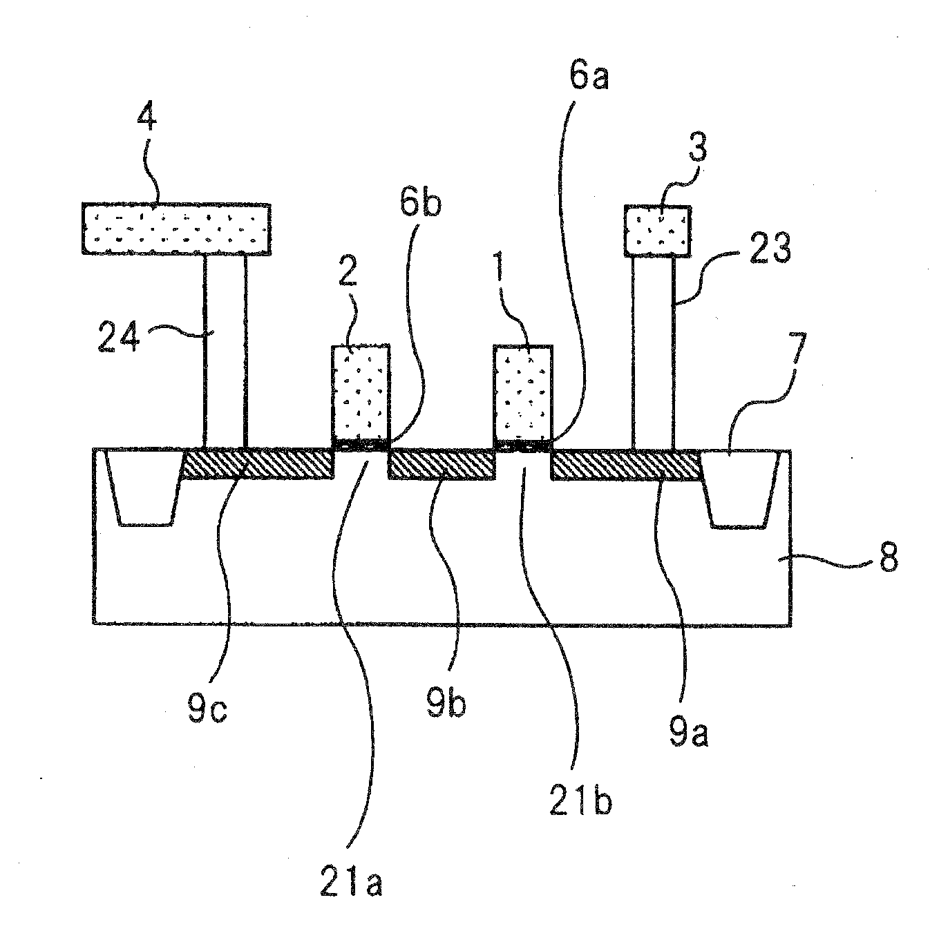
[0030]In the antifuse of the present exemplary embodiment, an active area is provided on a surface of P-type semiconductor substrate 8, which includes diffusion layers 9a to 9c in which a N-type impurity is introduced, and channel areas 21a and 21b, and the active area is divided to four areas. The divided areas are referred to as divided areas 5a to 5d respectively. Isolation portion 7 such as the STI (Shallow Trench Isolation) is provided between the divided areas.

[0031]As illustrated in FIG. 3A, two wirings among four divided...

second exemplary embodiment

[0058]While one wiring is selected from the break selection wiring in the first exemplary embodiment, a plurality of wirings are selected as the break selection wiring in the present exemplary embodiment.

[0059]A configuration of the antifuse of the present exemplary embodiment will be described.

[0060]Unlike the first exemplary embodiment, it is desirable that the wiring resistance of drain electrode 2 of the present exemplary embodiment is as small as possible. Thus, the dopant density in the Poly-Si of drain electrode 2 is adjusted so that the wiring resistance becomes smaller as in the gate electrode of the MOS transistor. It is desirable that the shape of the pattern is a straight line so that the resistance value does not become larger according to the length. Meanwhile, since other configurations are the same as those of the first exemplary embodiment, a detailed description will be omitted.

[0061]Next, a method for writing information into the antifuse of the present exemplary ...


PUM


Abstract

An antifuse element includes a plurality of MOS transistors; a first electrode to which source electrodes of the plurality of MOS transistors are commonly connected; a second electrode to which gate electrodes of the plurality of MOS transistors are commonly connected; a third electrode to which at least one of drain electrodes of the plurality of MOS transistors is capable of being connected; and an insulation film provided between the drain electrodes of the plurality of MOS transistors and the third electrode, wherein the insulation on at least one position in said insulation film and that corresponds to one of the drain electrodes is broken down.

Description

[0001]This application is based upon and claims the benefit of priority from Japanese Patent Application No. 2007-286131 filed on Nov. 2, 2007, the content of which is incorporated by reference.BACKGROUND OF THE INVENTION[0002]1. Field of the Invention[0003]The present invention relates to an antifuse element for changing a circuit connection in a semiconductor device, and a method for setting the antifuse element.[0004]2. Description of Related Art[0005]In a semiconductor memory, a fuse is used to improve the production yield by substituting, with a spare substitution cell (redundant cell), a defective memory cell induced because of a foreign particle during manufacturing or because of an irregular memory cell whose refresh characteristic is irregular because of production fluctuation of a DRAM (Dynamic Random Access Memory). The fuse is also used in a circuit for adjusting the reference voltage in a reference voltage generating circuit in a semiconductor memory chip. Such a fuse i...

Claims


Application Information

Patent Timeline
Patent Type & Authority Applications(United States)
IPC IPC(8): H01L29/00H01H85/00
CPCH01L21/823462H01L27/112H01L27/0203H01L23/5252H01L2924/0002H10B20/00H01L2924/00
Inventor MORIWAKI, YOSHIKAZU
Owner ELPIDA MEMORY INC
Why Eureka
Try Eureka