Mounting structure of electronic component

a technology of mounting structure and electronic component, which is applied in the manufacture of printed circuits, printed circuit aspects, basic electric elements, etc., can solve the problems of inability to obtain sufficient bonding strength, contact defect, fluctuation in distance between lands and bump electrodes, etc., to improve the reliability of conductive connection, improve bonding strength, and reduce mounting costs

Inactive Publication Date: 2009-05-07
138 EAST LCD ADVANCEMENTS LTD
View PDF7 Cites 2 Cited by
  • Summary
  • Abstract
  • Description
  • Claims
  • Application Information

AI Technical Summary

Benefits of technology

[0013]An advantage of the invention is to provide a mounting structure of an electronic component that exhibits improved bonding strength between a bump electrode and a terminal on a substrate, as well as an improved reliability of a conductive connection, while allowing for the cost reduction for mounting.
[0014]According to an aspect of the invention, a mounting structure of an electronic component includes: a substrate having a terminal and the electronic component which is mounted on the substrate; and a bump electrode included in the electronic component. This bump electrode has an underlying resin provided on an active surface of the electronic component, and a conductive film covering part of a surface of the underlying resin and exposing the rest so as to be electrically continued to an electrode terminal. In this mounting structure, the conductive film of the bump electrode makes direct conductive contact with the terminal, and the underlying resin of the bump electrode elastically deforms so that at least part of an exposed area which is exposed without being covered by the conductive film directly adheres to the substrate. Further, the substrate and the electronic component retain a state of the bump electrode making conductive contact with the terminal by adhesivity of the exposed area of the underlying resin to the substrate.
[0015]According to this mounting structure of an electronic component, the bump electrode includes the underlying resin and the conductive film covering part of the surface of the underlying resin. A pressure applied on the terminal on the substrate easily presses the bump electrode and yields an elastically (compressively) deformed state of the underlying resin. Elastic restoring force (repelling force) increases the bonding strength between the bump electrode and the terminal, the elastic restoring force being generated in the bump electrode against the terminal of the substrate due to the elastic deformation of the internal resin in the bump electrode, thereby improving the reliability of a conductive connection.
[0016]The underlying resin elastically deforming in a state of at least part of the exposed area directly adhering to the substrate as described retains the state in which the bump electrode makes direct conductive contact with the terminal by the adhesivity of this exposed area to the substrate. This eliminates the necessity to dispose adhesives such as underfills between the substrate and the electronic component. Consequently, this allows for reducing a cost of materials for adhesives such as underfills, as well as a production cost due to the elimination of a process of disposing such adhesives, thereby resulting in a reduction in a cost for mounting.
[0017]In this case, the the bump electrode and the terminal may be provided in plurality so as to include at least two bump electrodes and at least two terminals, each of the at least two bump electrodes corresponding to one of the at least two terminals so as to be bonded together. Moreover, the at least two terminals may each have a top surface with a different height so as to be bonded to the at least two bump electrodes, and the at least two bump electrodes may be bonded to the at least two terminals in a state in which a height fluctuation of the at least two terminals is absorbed by the underlying resin elastically deforming in proportion with the height of each of the at least two terminals to be bonded.
[0018]If the terminal is formed on the substrate in plurality, the top surfaces (bonding surface) of the terminals may fluctuate in height (level), due to causes such as: concaves and convexes or warping of the substrate; and process variation in the manufacturing of terminals. This causes the top surfaces of the plurality of terminals to have different distances relative to the bump electrodes.

Problems solved by technology

However, since lands and bump electrodes are generally formed with metal, a mispositioning during bonding and a misalignment caused by a low aligning precision of lands and bump electrodes could result in a contact defect (conductive defect) originating from insufficient bonding strength between these lands and bump electrodes.
Moreover, there has been a possibility that a warping of electronic components such as substrates and ICs as well as a fluctuation in setting the height of lands and bump electrodes causes a fluctuation in distance between lands and bump electrodes.
This could result in an inability to obtain sufficient bonding strength between the bump electrodes and the terminals, causing a contact defect (conductive defect).
However, while the slipping, the sliding, and the inclination of connecting electrodes (bump electrode) arranged over the metal conductive layer are prevented by the anchor effect that originates from the concavities and convexities of the metal conductive surface, the above-mentioned print circuit board does not have a structure that increases the bonding strength between the metal conductive substrate and the connecting electrode.
Further, the structure does not increase the bonding strength of the pluralities of electrodes.
Consequently, occurrences of mispositioning during bonding and misalignment of electrodes (lands and bump electrodes) caused by low aligning precision thereof may still result in a contact defect (conductive defect) originating from insufficient bonding strength of these electrodes.
This means that, if the distance between the lands and the electrodes were uneven as described above, the connecting electrodes would have a low capability in absorbing the distance deviation by the elastic deformation, and therefore the bonding strength between these electrodes would be insufficient.
For this reason, the contact defect (conductive defect) may still occur as well.
Moreover, when coupling the substrate and the electronic component through the pluralities of bump electrodes and terminals, the substrate including terminals with uneven heights and the electronic component including bump electrodes, a fluctuation in the distance from the bump electrodes to the terminals prior to their bonding makes it difficult to couple all the bump electrodes and all the terminals in a preferable strength.
Moreover, when coupling the electronic component and the substrate at the pluralities of bump electrodes and terminals, the electronic component including the bump electrodes with uneven height and the substrate including terminals, a fluctuation in the distance between the bump electrodes and the terminals prior to their bonding makes it difficult to couple every bump electrode to a corresponding terminal in a preferable strength.

Method used


Image

  • Mounting structure of electronic component
  • Mounting structure of electronic component
  • Mounting structure of electronic component

Examples


first embodiment

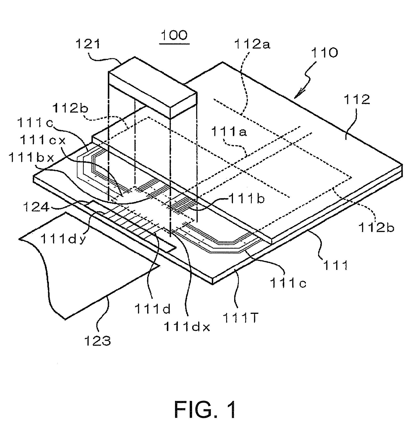
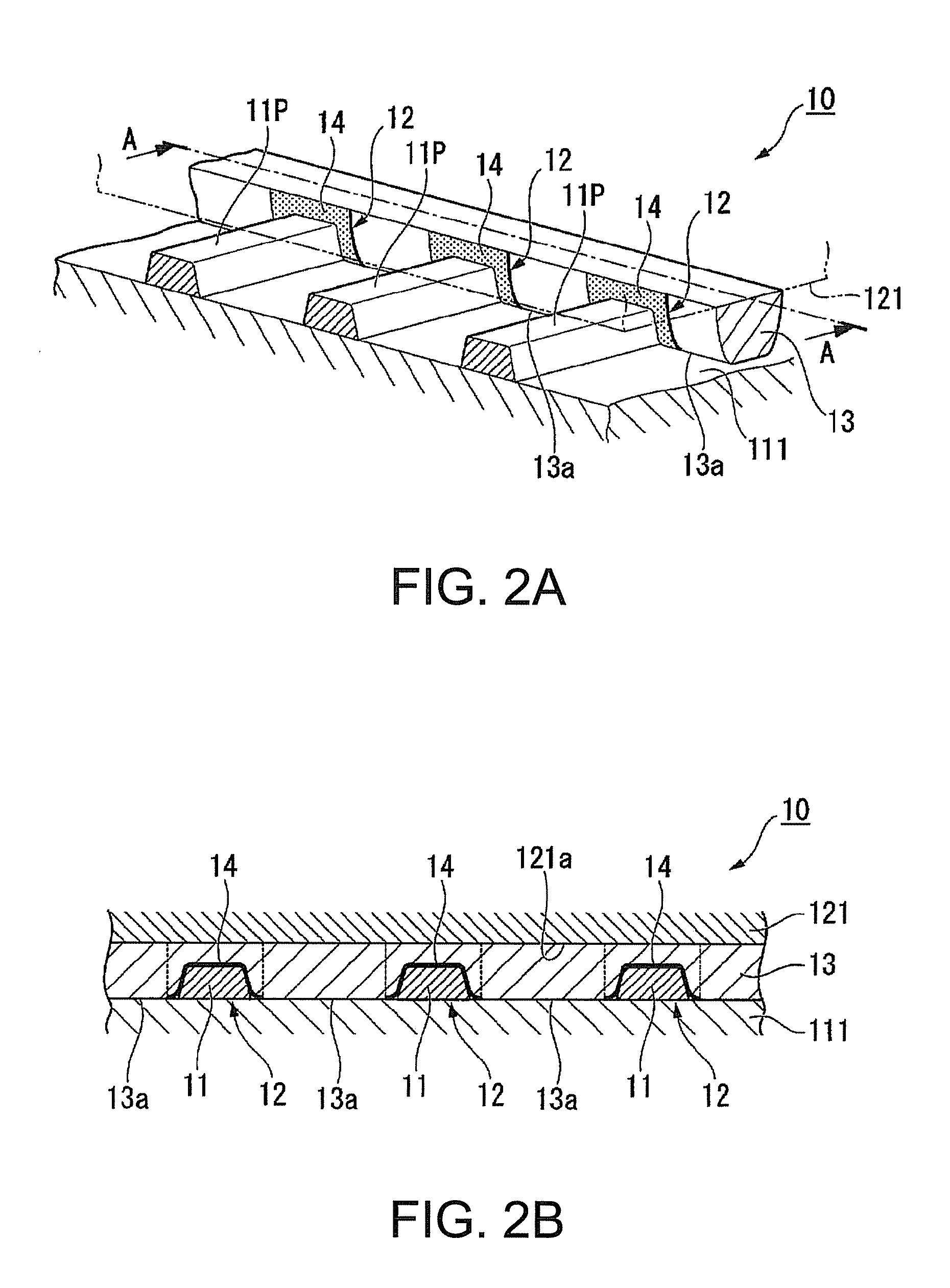
[0065]FIG. 2A is a magnified perspective view illustrating main parts of a first embodiment, which is the mounting structure of the electronic component 121 in the liquid crystal device 100. FIG. 2B is a sectional view along A-A line in FIG. 2A. 11P in FIGS. 2A and 2B indicates a wiring pattern provided on the substrate 111, and the number 11 indicates each terminal installed in the wirings, i.e. any of the above-described terminals 111bx, 111cx, and 111dx. In this embodiment, the terminals 11 have a relatively large film thickness, which therefore means that the height of the terminals 11 is large, with a transverse sectional surface thereof being approximately trapezoid. The number 12 indicates each bump electrode provided to the electronic component 121.

[0066]In these embodiments, as illustrated in FIG. 2A and sectional views of FIGS. 3A and 3B, each of the bump electrodes 12 has underlying resin 13 and a conductive film 14. The underlying resin 13 is shaped approximately like a ...

second embodiment

[0081]In the second embodiment shown in FIGS. 5A and 5B, the fluctuation in height of the terminals 11a and 11b originates from the process variation in the manufacturing of the terminals 11. Here, since the terminals 11 are formed with an additive process (plating deposition), they have a relatively thick film thickness, which means that the height of the terminals 11 is large, and a transverse sectional surface of the terminals 11 is approximately trapezoid. The terminals 11 may be formed in other shapes such as: one formed by etching with the transverse sectional surface being rectangular as shown in FIG. 6A; a thin film formed by sputtering as shown in FIG. 6B; and an approximately like a barrel vault formed by printing as shown in FIG. 6C.

[0082]The terminal 11a and the terminal 11b with different heights are bonded to two of the bump electrodes 12 corresponding thereto while absorbing the height fluctuation (difference) of the terminals 11a and 11b, and in this state, the expos...


PUM


Abstract

A mounting structure of an electronic component includes: a substrate having a terminal and the electronic component which is mounted on the substrate; and a bump electrode included in the electronic component. This bump electrode has an underlying resin provided on an active surface of the electronic component, and a conductive film covering part of a surface of the underlying resin and exposing the rest so as to be electrically continued to an electrode terminal. In this mounting structure, the conductive film of the bump electrode makes direct conductive contact with the terminal, and the underlying resin of the bump electrode elastically deforms so that at least part of an exposed area which is exposed without being covered by the conductive film directly adheres to the substrate. Further, the substrate and the electronic component retain a state of the bump electrode making conductive contact with the terminal by adhesivity of the exposed area of the underlying resin to the substrate.

Description

BACKGROUND[0001]1. Technical Field[0002]The present invention relates to a mounting structure of an electronic component.[0003]2. Related Art[0004]Mounting techniques are used in mounting, on a substrate, electronic components such as semiconductor integrated circuit, when manufacturing liquid crystal devices and a circuit substrate mounted on various electronic apparatuses. A liquid crystal display device, for instance, includes an integrated circuit (IC) chip for liquid crystal drive so as to drive the liquid crystal panel. This IC chip for liquid crystal drive may also be mounted directly on a glass substrate that constitutes the liquid crystal panel, or, may be mounted on a flexible substrate (FPC) which is mounted on the liquid crystal panel. A mounting structure mounted by the former technique is called a chip on glass (COG) structure, and a mounting structure mounted by the latter is called a chip on flexible print circuit (COF) structure. In addition to these mounting struct...

Claims


Application Information

Patent Timeline
Patent Type & Authority Applications(United States)
IPC IPC(8): H01L23/52
CPCH01L2224/16H01L2924/01046H01L2924/01078H01L2924/01079H01L2924/14H01L2924/19041H01L2924/3511H05K3/325H05K2201/0382H05K2201/10674H05K2201/10977H05K2201/10984H05K3/305H01L24/02H01L24/05H01L24/13H01L2224/023H01L2224/05001H01L2224/05024H01L2224/05026H01L2224/05548H01L2224/05624H01L2224/05644H01L2224/05655H01L2224/05664H01L2224/05666H01L2224/05671H01L2224/05684H01L2224/13008H01L2224/1319H01L2924/0001H01L2924/00014H01L2224/05099H01L2224/02
Inventor HASHIMOTO, NOBUAKI
Owner 138 EAST LCD ADVANCEMENTS LTD
Why Eureka
Try Eureka