
Mask pattern correction method for manufacture of semiconductor integrated circuit device

a semiconductor integrated circuit and mask pattern technology, applied in the field of mask pattern correction method for manufacturing of semiconductor integrated circuit devices, can solve the problems of large error sum, semiconductor devices cannot normally operate, and the quota of manufacturing errors allowed in each step also becomes small

Inactive Publication Date: 2009-05-07
KK TOSHIBA
View PDF14 Cites 10 Cited by
  • Summary
  • Abstract
  • Description
  • Claims
  • Application Information

AI Technical Summary

Problems solved by technology

However, for example, all the errors accidentally occur to make a pattern thinner than the design values, and the absolute value of the sum of errors becomes large in some cases.
This poses a nonnegligible problem because if the discrepancy between the design values and the dimensions of the finally formed pattern grows, the semiconductor device cannot normally operate.
Accordingly, the quota of manufacturing errors allowable in each step also becomes small, and the tolerance is approaching the working limit.
However, even when the layout does not change, generated dimensional errors change due to the manufacturing errors of a photomask or errors generated in succeeding steps.
Hence, in the OPC, uncorrectable errors pose a problem, as described in. e.g., Jpn. Pat. Appln. KOKAI Publication No. 2002-148779.

Method used


Image

  • Mask pattern correction method for manufacture of semiconductor integrated circuit device
  • Mask pattern correction method for manufacture of semiconductor integrated circuit device
  • Mask pattern correction method for manufacture of semiconductor integrated circuit device

Examples


first embodiment

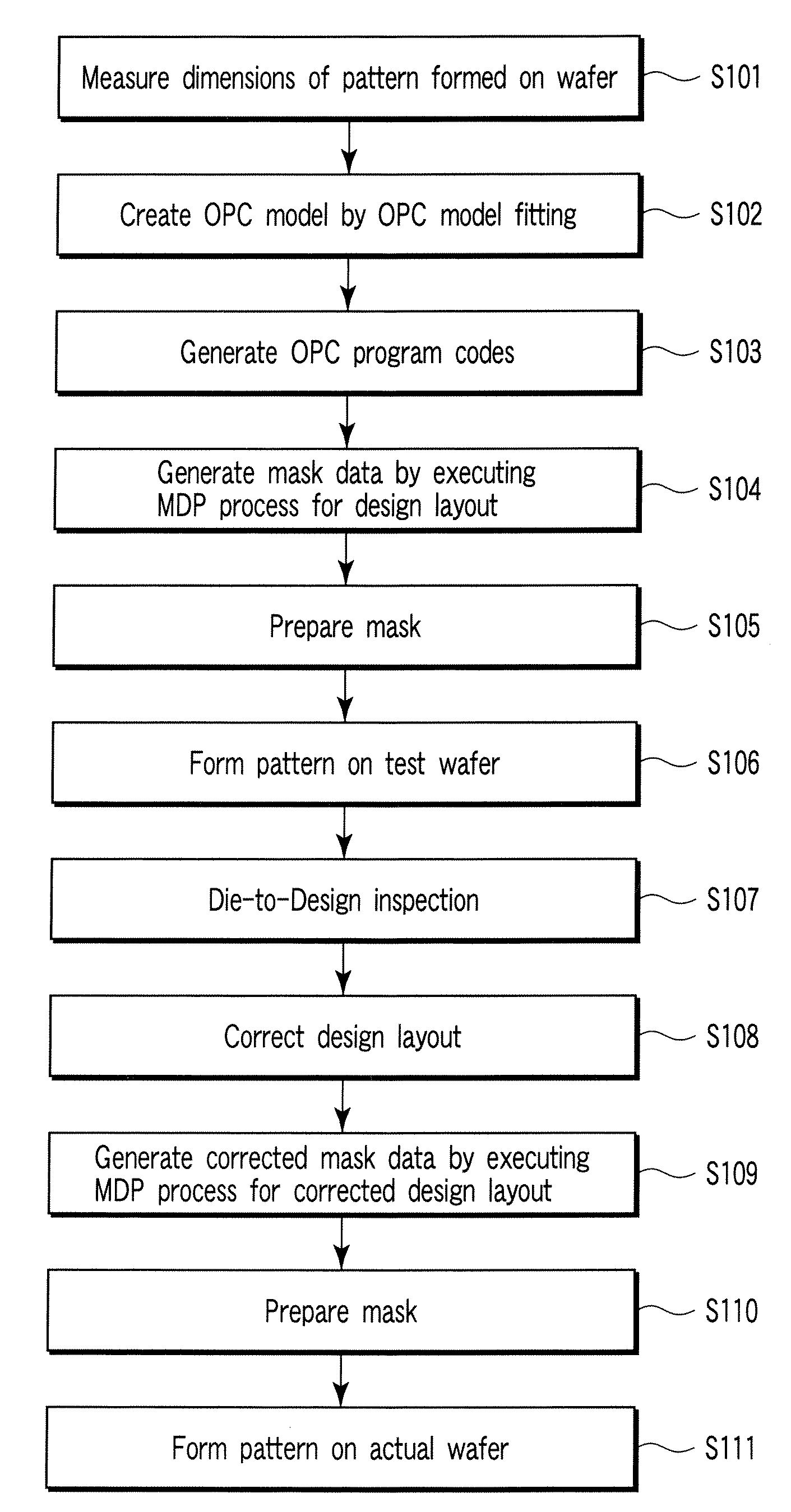
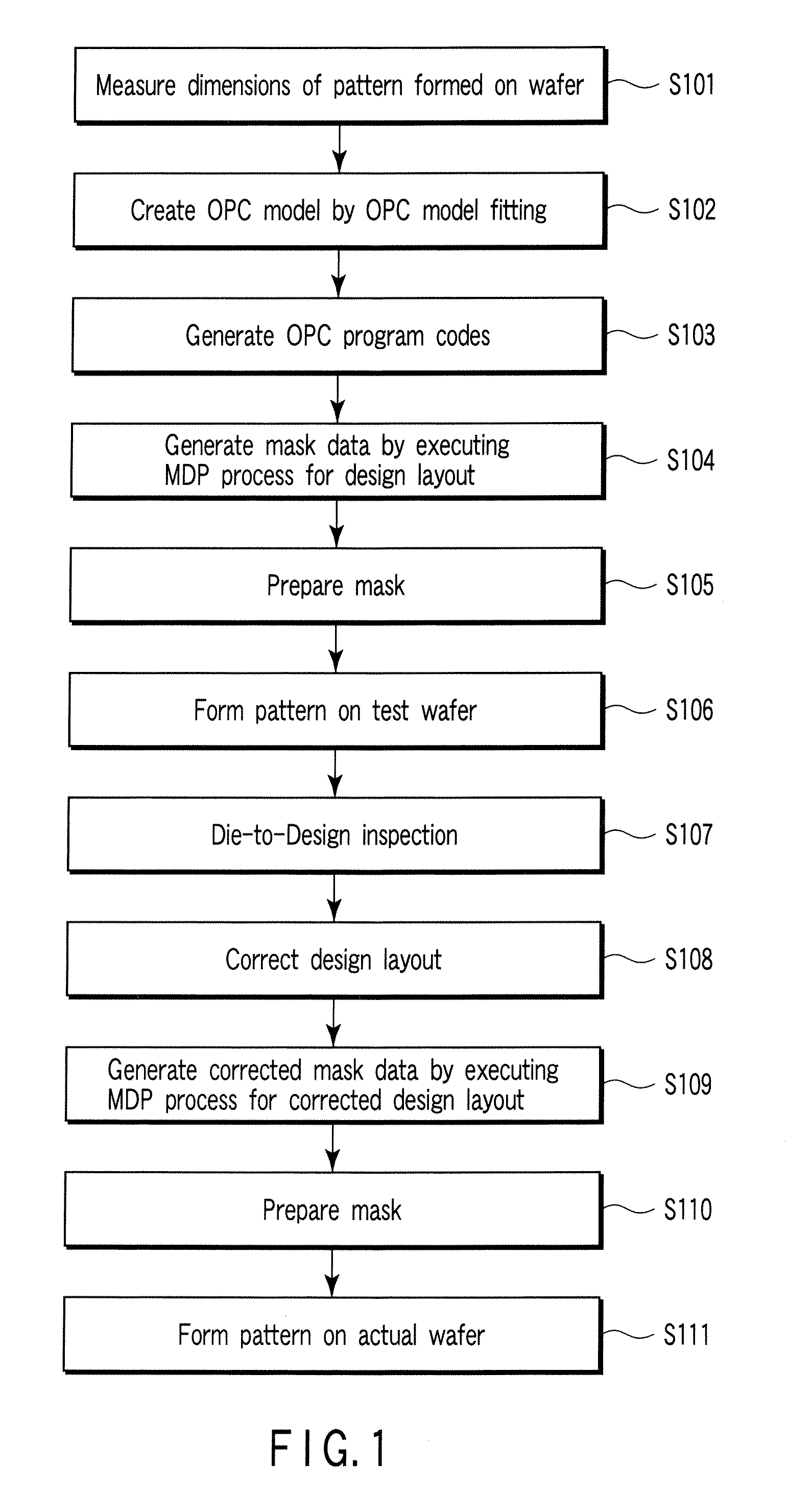
[0040]As described above, a mask pattern correction method according to the present invention comprises steps of generating mask data from a design layout by executing a mask data process including optical proximity correction based on an optical proximity correction model, forming a pattern on a major surface of a test semiconductor substrate by using a mask prepared based on the mask data, measuring a dimensional difference between the design layout and the pattern, generating a corrected design layout by correcting the design layout, at a portion with the dimensional difference of the design layout, by a magnitude of the dimensional difference in a direction in which dimensions of the pattern equal those of the design layout, and generating corrected mask data from the corrected design layout by executing the mask data process including the optical proximity correction based on the optical proximity correction model.

second embodiment

[0041]A design layout correction method according to the present invention comprises steps of generating mask data from a design layout, forming a pattern on the major surface of a test semiconductor substrate by using a mask prepared based on the mask data, measuring the dimensional difference between the design layout and the pattern, and generating a corrected design layout by correcting the design layout, at a portion with the dimensional difference of the design layout, by the magnitude of the dimensional difference in a direction in which the dimensions of the pattern equal those of the design layout.

[0042]A mask manufacturing method according to a embodiment aspect of the present invention comprises steps of preparing a mask based on mask data which is generated from a design layout by executing a mask data process including optical proximity correction based on an optical proximity correction model, obtaining information of a dimensional difference between the design layout ...

fifth embodiment

[0044]A semiconductor mask data generating apparatus according to the present invention comprises means for generating mask data from a design layout, means for obtaining information of the dimensional difference between the design layout and a pattern formed on the major surface of a test semiconductor substrate by using a mask prepared based on the mask data, and means for generating semiconductor mask data from a corrected design layout generated by correcting the design layout, at a portion with the dimensional difference of the design layout, by the magnitude of the dimensional difference in a direction in which the dimensions of the pattern equal those of the design layout.

[0045]As described above, according to one aspect of this invention, it is possible to provide a semiconductor integrated circuit device manufacturing method, mask manufacturing method, semiconductor mask data generating apparatus, mask pattern correction method, and design layout correction method capable o...


PUM


Abstract

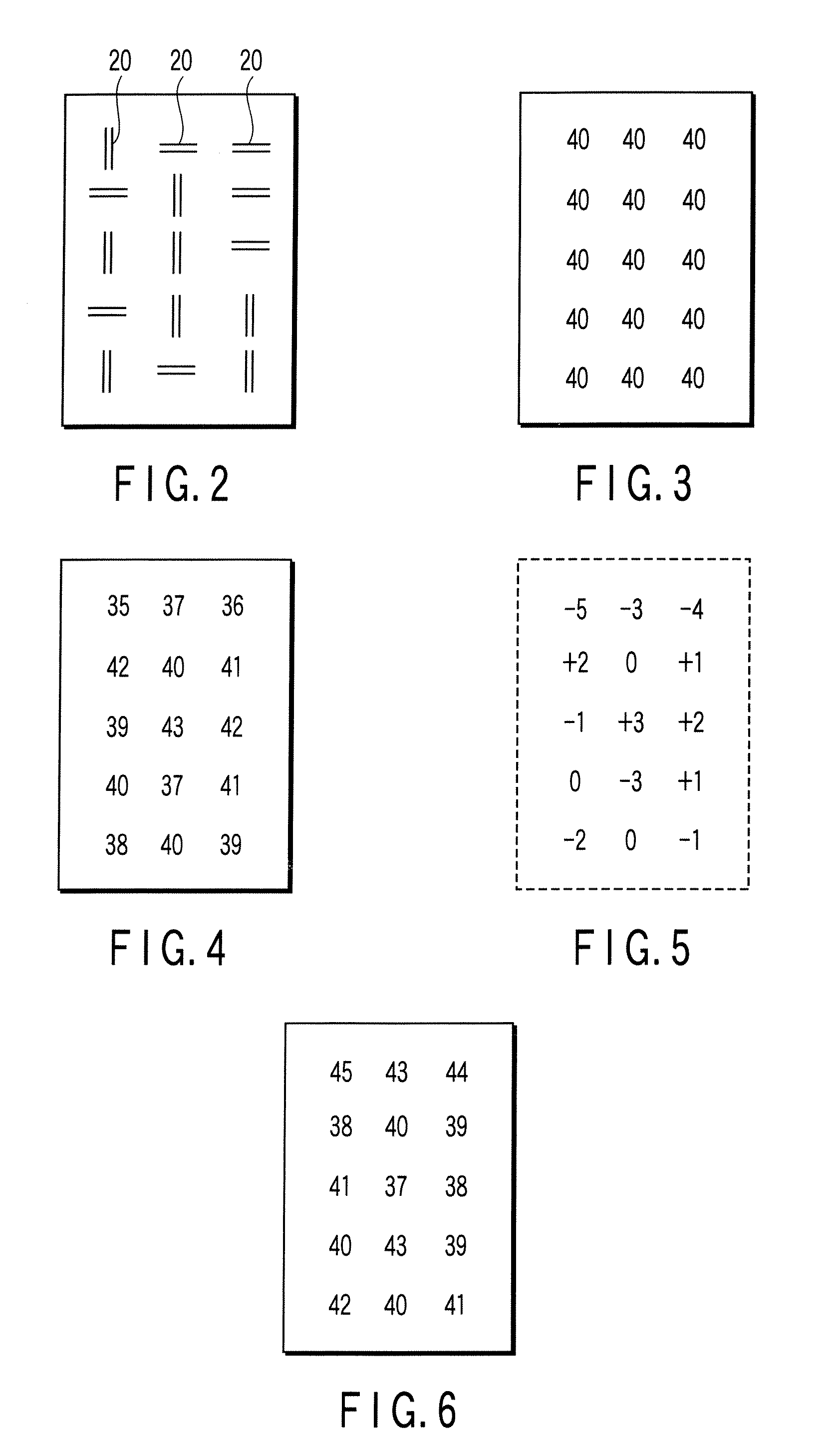
Mask data is generated from a design layout by executing a mask data process including optical proximity correction. A pattern is formed on the major surface of a test semiconductor substrate by using a mask prepared from the mask data. The dimensional difference between the design layout and the pattern is measured. The design layout is corrected, at a portion with the dimensional difference of the design layout, by the magnitude of the dimensional difference in a direction in which the dimensions of the pattern equal those of the design layout, thereby generating a corrected design layout. Corrected mask data is generated from the corrected design layout by executing the mask data process including the optical proximity correction. A pattern is formed on the major surface of a semiconductor substrate by using a corrected mask prepared from the corrected mask data.

Description

CROSS-REFERENCE TO RELATED APPLICATIONS[0001]This application is based upon and claims the benefit of priority from prior Japanese Patent Application No. 2006-327239, filed Dec. 4, 2006, the entire contents of which are incorporated herein by reference.BACKGROUND OF THE INVENTION[0002]1. Field of the Invention[0003]The present invention relates to a mask pattern correction method for manufacture of a semiconductor integrated circuit device. The present invention also relates to a mask manufacturing method and semiconductor integrated circuit device manufacturing method using the correction method.[0004]2. Description of the Related Art[0005]In manufacturing a semiconductor integrated circuit device, a resist pattern is formed by lithography, an underlying film is worked by etching, and a circuit pattern is formed on a wafer. In this pattern formation technology, it is demanded to form, on a wafer, a pattern with dimensions accurately conforming to design values.[0006]One of the tech...

Claims


Application Information

Patent Timeline
IPC IPC(8): G06F17/50G03F1/36G03F1/68G03F1/70G03F1/72H01L21/027
CPCG03F1/14G03F7/70625G03F1/36G03F1/144G03F1/68
Inventor TAKAHATA, KAZUHIRO
Owner KK TOSHIBA
Learn More