Method of producing a suspended membrane device

a technology of suspended membrane and production method, which is applied in the field of method of producing suspended membrane devices, microsensors, etc., can solve the problems of not being able to obtain a precise characterisation of the dimensions of the structure produced, and the inability to use time as a dimensional control parameter for the suspended structure produced, so as to reduce the degradation of mechanical properties of the suspended structure and improve the attachment of the structure produced. , the effect of improving the precision

Active Publication Date: 2009-05-14
COMMISSARIAT A LENERGIE ATOMIQUE ET AUX ENERGIES ALTERNATIVES
View PDF12 Cites 19 Cited by
  • Summary
  • Abstract
  • Description
  • Claims
  • Application Information

AI Technical Summary

Benefits of technology

[0009]Thus there is a need to propose a new method of producing a suspended membrane, which eliminates or reduces the disadvantages of the methods of the prior art, i.e., which offers improved precision in the production of the suspended membrane, e.g., with respect to the dimensions and shape of the membrane produced, thereby making it possible to obtain suspended membranes of any shape, limiting degradation of the mechanical properties of this membrane due to the production method, and improving the attachments of the structure produced.

Problems solved by technology

However, it is sometimes necessary to produce membranes which do not comprise anchoring studs distributed thereunder.
In particular, this method has the disadvantage of using time as a dimensional control parameter for the suspended structure produced.
Such being the case, and given that the etch rate depends on the pH of the etching agent and that, for a single etching agent, this rate depends on the temperature and composition of the etched dielectric, this method does not make it possible to obtain a precise characterisation of the dimensions of the structure produced.

Method used


Image

  • Method of producing a suspended membrane device
  • Method of producing a suspended membrane device
  • Method of producing a suspended membrane device

Examples


first embodiment

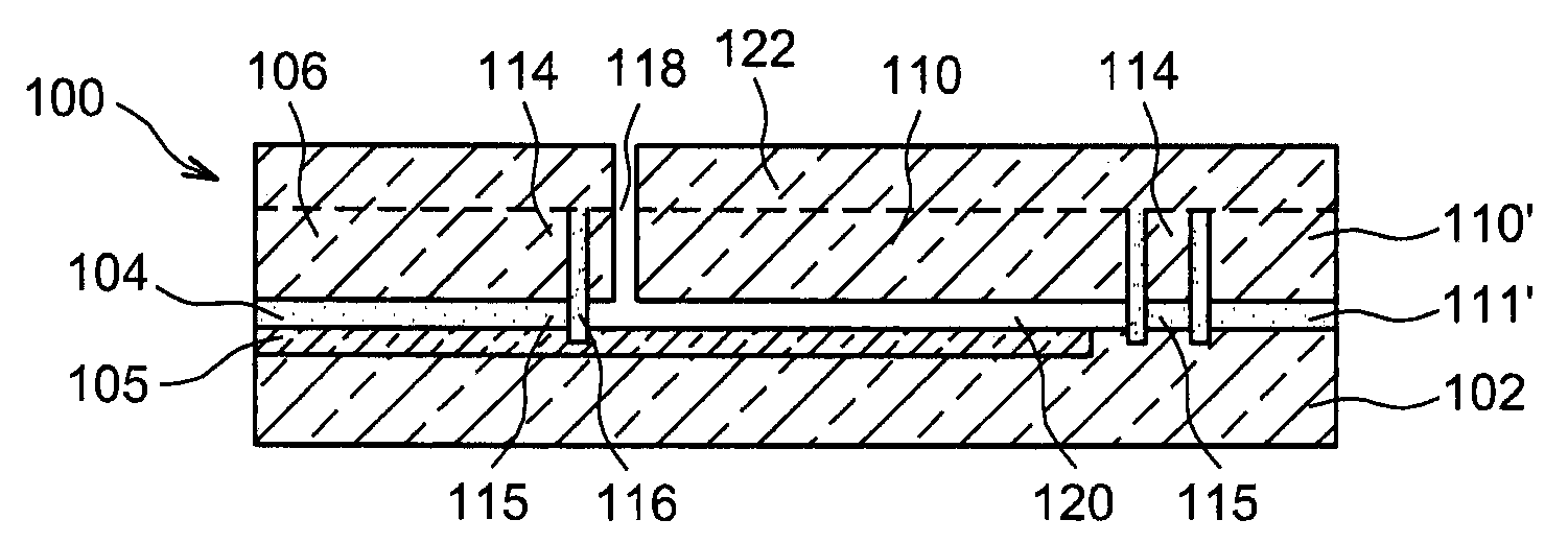
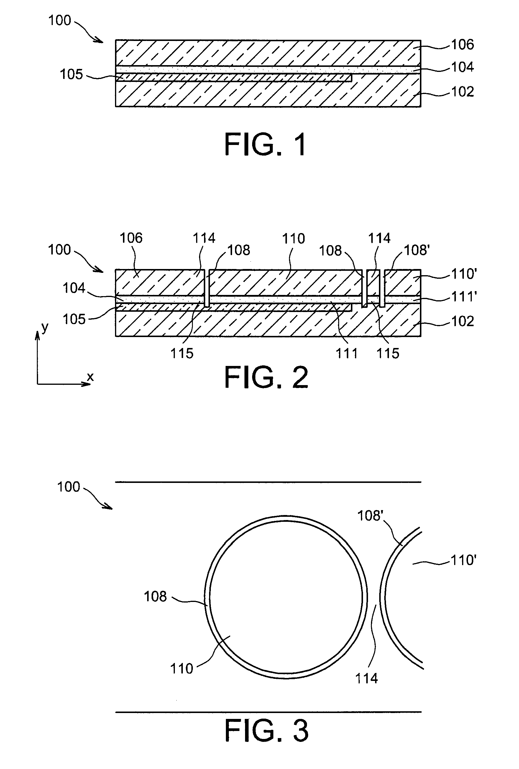
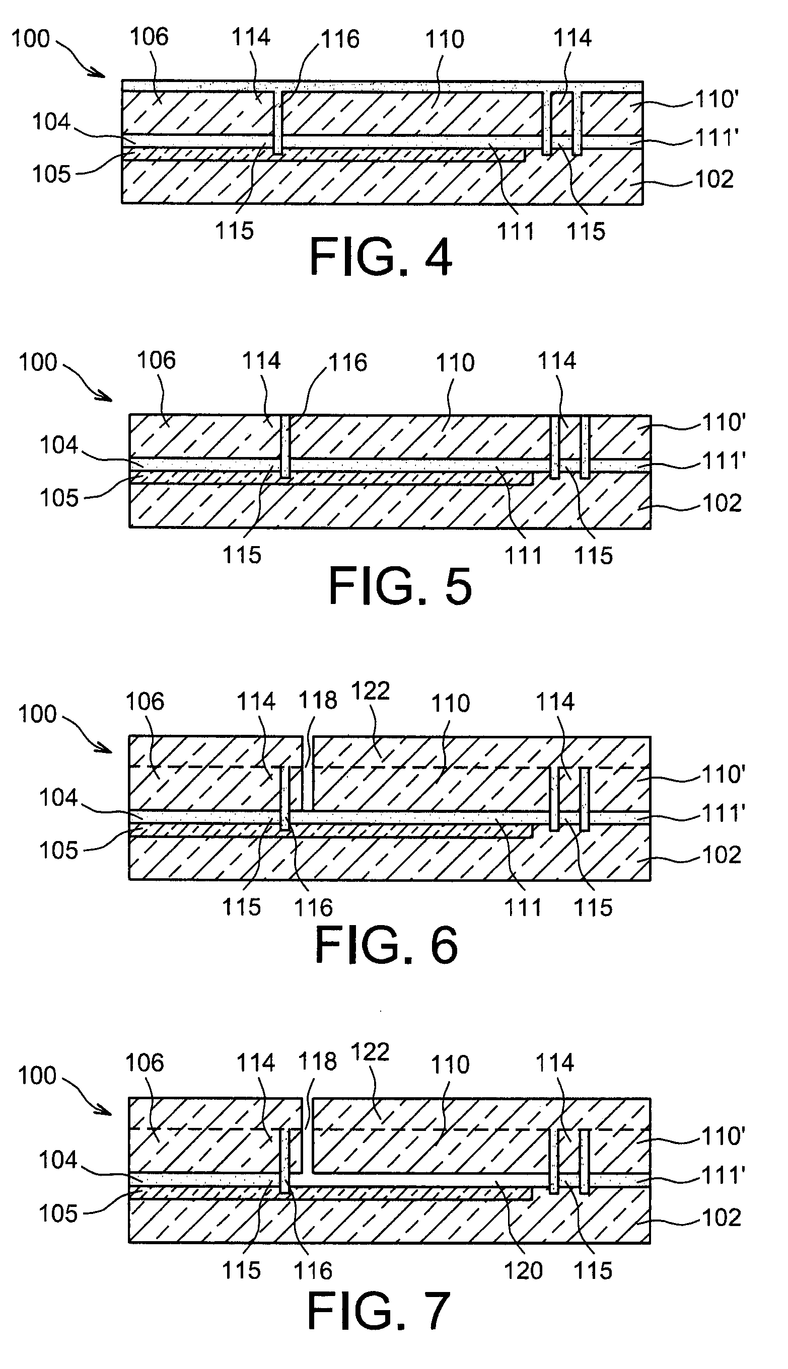
[0046]Reference is first made to FIGS. 1 to 7, which show the steps of a method for producing a suspended membrane device 100 according to a

[0047]The device 100 is produced from semiconductor-based substrate 102 such as silicon, upon which are stacked a dielectric layer 104, e.g., containing SiO2 and forming a sacrificial layer having a thickness equal to approximately 1 μm, or more generally between approximately 0.1 μm and 3 μm, and a thin layer 106 containing a semiconductor material, e.g., monocrystalline silicon. In an alternative, layer 106 may contain a semiconductor material other than silicon, e.g., such as SiC (silicon carbide) or a piezoelectric material such as LiNbO3 (lithium niobate) or BaTiO3 (barium titanate). In this case, the semiconductor layer 106 has a thickness of less than approximately 10 μm, or of between approximately 0.1 μm and several tens of micrometres, or less than approximately 100 μm. In this first embodiment, the substrate 102, the sacrificial layer...

third embodiment

[0087]As shown in FIG. 34, the portion 311 of the sacrificial layer 304 defined by the trench 308 is then etched. In this third embodiment, it is the epitaxially grown material 312, in this case silicon, which forms the etch stop material. This etching may be carried out with an HF-based aqueous solution.

second embodiment

[0088]As in the second embodiment, the opening 314 is plugged by depositing and etching a material 316 such as phosphosilicate glass (PSG) (FIG. 35). Creep may then be produced by PSG annealing at a temperature greater than 1000° C.

[0089]Ion implantation is then carried out, forming piezoelectric gauges 318 in the epitaxially grown layer 312 (FIG. 36). The device 300 is then passivated by depositing a passivation layer 320 (FIG. 37).

[0090]Contact holes 322 are then made in the passivation layer 320, in the vicinity of the gauges 318 (FIG. 38).

[0091]The device 300 is then completed by making metal interconnecting tracks 324, as shown in FIG. 39, which come into contact with the gauges 318.

[0092]In the three embodiments described, each trench defining a portion of the semiconductor layer intended to form a suspended membrane of the device is entirely filled with the etch stop material intended for stopping the etching of a sacrificial material. In an alternative of these three embodim...


PUM


Abstract

A method for producing a device with at least one suspended membrane, comprising at least the following steps:
    • producing a trench through a first sacrificial layer and a second layer deposited on the first sacrificial layer, the trench completely surrounding at least a portion of the first sacrificial layer and at least a portion of the second layer,
    • filling all or a portion of the trench with at least one material capable of resisting at least one etching agent,
    • etching said portion of the first sacrificial layer with said etching agent through at least one opening made in the second layer,
    • said portion of the second layer forming at least one portion of the suspended membrane.

Description

TECHNICAL FIELD[0001]This document relates to the field of MEMS (microelectromechanical systems) or NEMS (nanoelectromechanical systems) and, in particular, that of microsensors comprising surface technology-produced suspended elements.PRIOR ART[0002]Several methods currently exist which enable production of MEMS comprising suspended portions of material called suspended membranes.[0003]The document US 2004 / 0119125 describes a method of producing a surface MEMS structure from an SOI (silicon on insulator) substrate. Several openings are made through the silicon upper layer and the dielectric layer of the SOI substrate. An insulating and etch-resistant material is deposited in these openings, and then a silicon layer is grown epitaxially on the upper layer of silicon of the SOI substrate. The dielectric layer is then etched, thereby causing the epitaxially grown layer to rest on anchoring studs formed by the insulating material and connected to the lower layer of silicon of the SOI s...

Claims


Application Information

Patent Timeline
Patent Type & Authority Applications(United States)
IPC IPC(8): H01L21/00
CPCB81C2201/014B81C1/00158
Inventor REY, PATRICESALHI, MOUNA
Owner COMMISSARIAT A LENERGIE ATOMIQUE ET AUX ENERGIES ALTERNATIVES
Why Eureka
Try Eureka