
Semiconductor device and imaging capturing apparatus

Active Publication Date: 2009-06-04
SEMICON COMPONENTS IND LLC
View PDF9 Cites 4 Cited by
  • Summary
  • Abstract
  • Description
  • Claims
  • Application Information

AI Technical Summary

Benefits of technology

[0008]There is therefore today a demand for a semiconductor device provided with an anti-shake function, which may be employed in a wide range of applications and which can achieve high-speed processing.

Problems solved by technology

On the other hand, there are problems that, because the processing rate of a microcomputer decreases as the volume of signal processing increases, performing the processing required by the microcomputer in order to achieve higher functionality is more difficult in apparatuses provided with an anti-shake function.
While integrating dedicated signal processing circuits (dedicated circuits) can effectively increase the processing rate, such integration of dedicated circuits requires redesign of the dedicated circuits each and every time the apparatus design is changed, and therefore significantly and undesirably increases manufacturing costs.

Method used


Image

  • Semiconductor device and imaging capturing apparatus
  • Semiconductor device and imaging capturing apparatus
  • Semiconductor device and imaging capturing apparatus

Examples


Embodiment Construction

[0026]A preferred embodiment of the present invention will be described in detail with reference to the accompanying drawings.

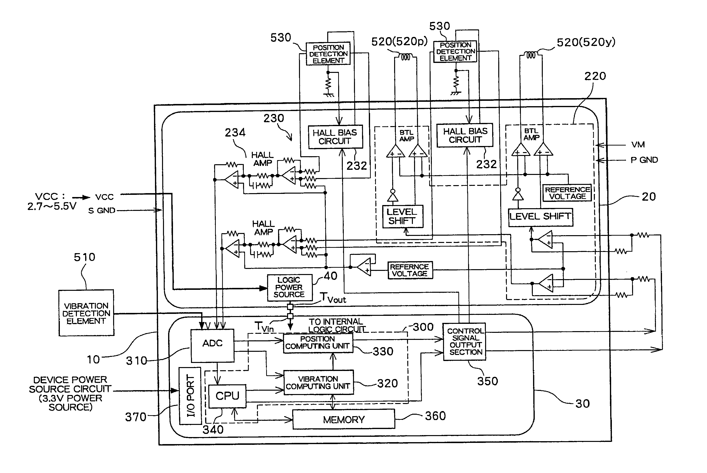
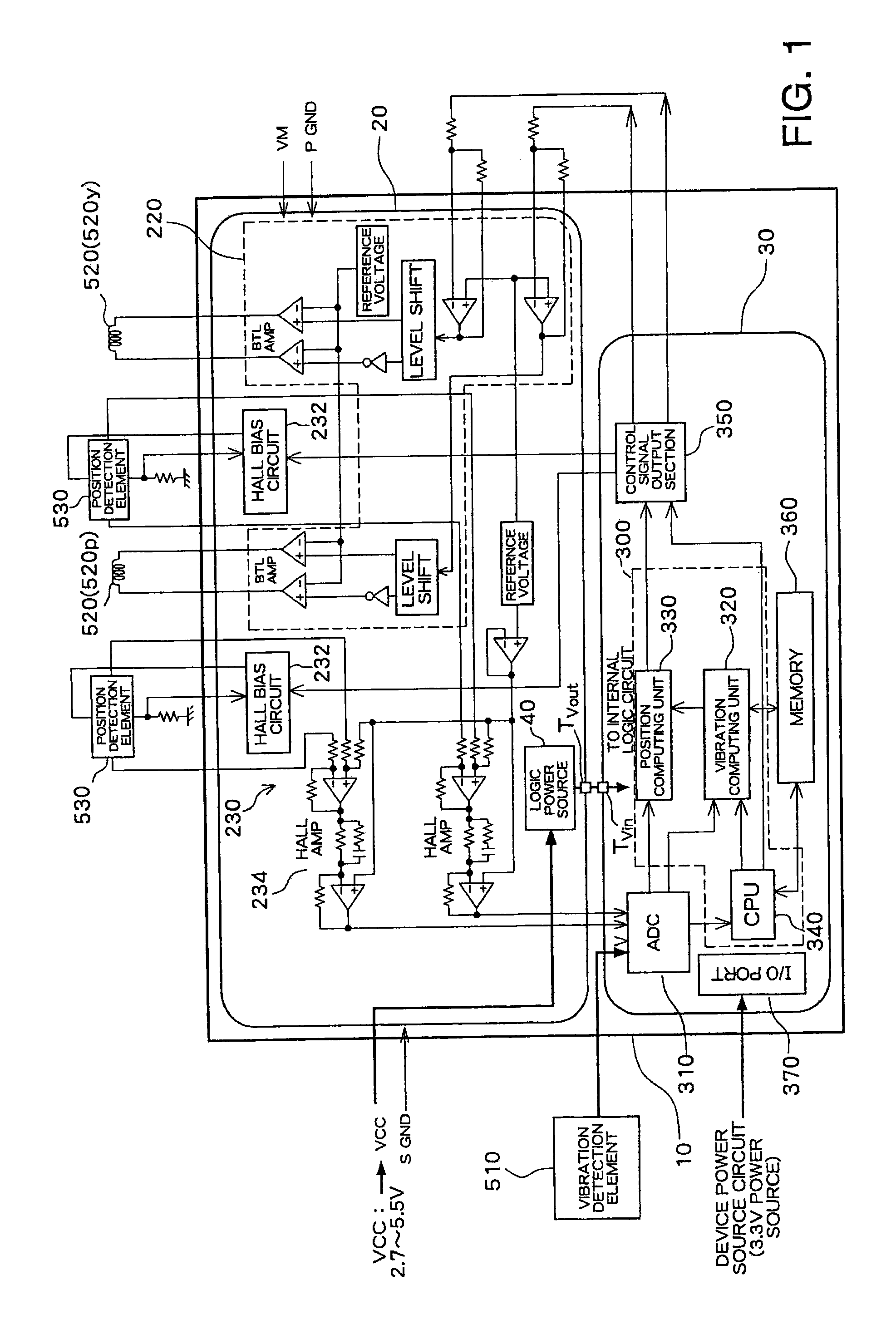
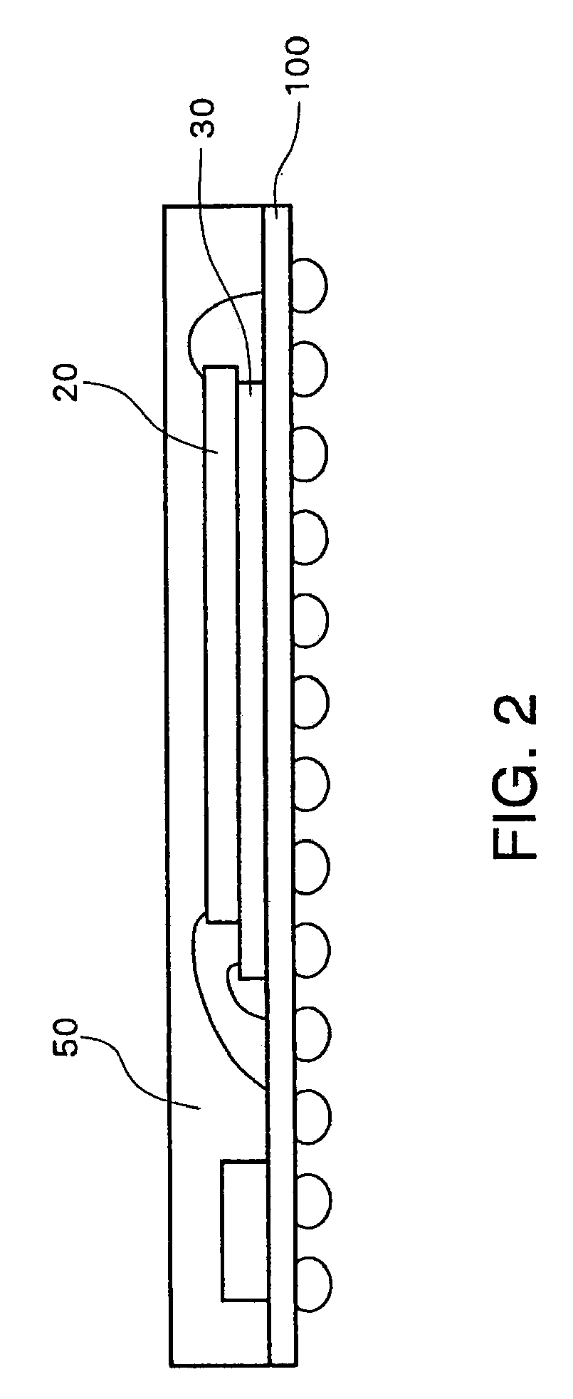
[0027]FIG. 1 schematically shows a structure of a semiconductor device 10 having an anti-shake function according to an embodiment of the present invention. The semiconductor device 10 is a semiconductor device having a multi-chip package (MCP) structure. More specifically, a driver chip 20 having analog circuits and a logic chip 30 having digital circuits are contained on a common substrate and sealed in a single package.

[0028]The semiconductor device 10 is used for executing processing for implementing an anti-shake function, such as for use in image capturing apparatuses including video cameras, digital still cameras, and so on, for example, namely, for image stabilization. Although applications of the anti-shake function of the present embodiment are not exclusive to image capturing apparatuses, the description of this embodiment will be based on an examp...


PUM


Abstract

A semiconductor device with an “anti-shake” function includes a logic chip having a digital circuit which obtains a value indicating the amount of vibration of device such as an imaging apparatus based on a vibration detection signal supplied from a vibration detection element to generate a correction signal. The logic chip includes a correction signal processing unit which generates the correction signal, and a control signal output unit which outputs a vibration control signal in accordance with the correction signal to a vibration correction control unit which executes vibration correction control for an optical component. The control signal output unit includes a plurality of types of signal output sections and outputs a vibration control signal corresponding to a driving unit from one signal output section selected from among the plurality of types of signal output sections.

Description

PRIORITY INFORMATION[0001]This application claims priority to Japanese Patent Applications No. 2007-307697 filed on Nov. 28, 2007, and No. 2008-244570 filed on Sep. 24, 2008 which are incorporated herein by reference in their entirety.BACKGROUND[0002]1. Technical Field[0003]The present invention relates to a semiconductor device which controls vibration, such as vibration caused by hand vibration or the like, and more particularly to a logic chip which processes a signal for anti-shake control.[0004]2. Related Art[0005]In image capturing apparatuses such as video cameras and digital still cameras, there has been a demand to prevent poor images caused by blurring of a subject image resulting from vibration, typically due to hand movement. In response to this demand, such apparatuses have come to be commonly provided with an “anti-shake” function. One known method for implementing an anti-shake function is by detecting vibration of the image capturing apparatus with respect to a subje...

Claims


Application Information

Patent Timeline
IPC IPC(8): H04N5/228
CPCG02B27/646G03B5/00H04N5/23287H04N5/23258H04N5/23261H04N5/23248H04N23/68H04N23/6812H04N23/6815H04N23/687
Inventor WATANABE, TOMOFUMI
Owner SEMICON COMPONENTS IND LLC
Learn More