IC with stably mounted chip

a technology of stably mounted and mounted chips, which is applied in the direction of electrical apparatus, semiconductor devices, semiconductor/solid-state device details, etc., can solve the problems that the ic does not meet the requirements of current electronic products, and achieve the effects of stable mounting, reduced overall thickness of the ic, and high processing and storage efficiency

Inactive Publication Date: 2006-01-26
TZU CHUNG HSING +1
View PDF3 Cites 0 Cited by
  • Summary
  • Abstract
  • Description
  • Claims
  • Application Information

AI Technical Summary

Benefits of technology

[0004] A primary object of the present invention is to provide an IC having a structure allowing at least one chip to stably mount therein and reduction of an overall thickness of the IC.
[0005] Another object of the present invention is to provide an IC having a structure allowing two chips to stably stack therein to enable high processing and storing efficiency and multiple functions.
[0006] To achieve the above and other objects, the IC with stably mounted chip according to the present invention includes a chip, a leadframe, a bridge, and an encapsulating compound. The bridge is a flat arch made of a sheet material and includes a horizontal fixing section and a supporting section downward extended from each end of the fixing section. The chip is adhered to a bottom side of the fixing section of the bridge. The leadframe includes a plurality of leads arranged at two opposite sides of the chip. The encapsulating compound is applied to cover the chip, the bridge, and inner portions of the leads to complete a compact IC having a stably mounted chip and a reduced overall thickness. And, an additional chip may be adhered to a top of the bridge, so that two chips are stably stacked in the IC.

Problems solved by technology

Moreover, since there is only one chip 10′ mounted in the IC in a manner not so stable to ensure a high processing and storing efficiency or to provide multiple functions, the IC does not satisfy the requirement of current electronic products.

Method used


Image

  • IC with stably mounted chip
  • IC with stably mounted chip
  • IC with stably mounted chip

Examples


Embodiment Construction

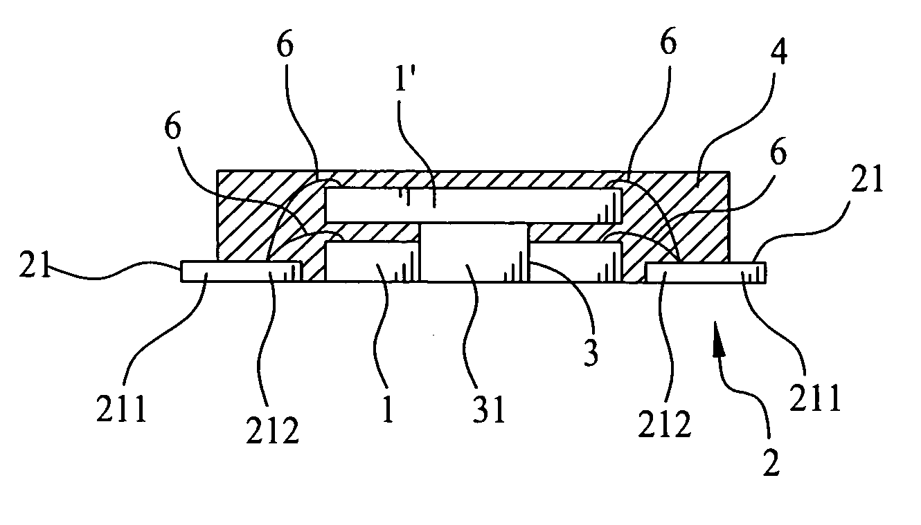
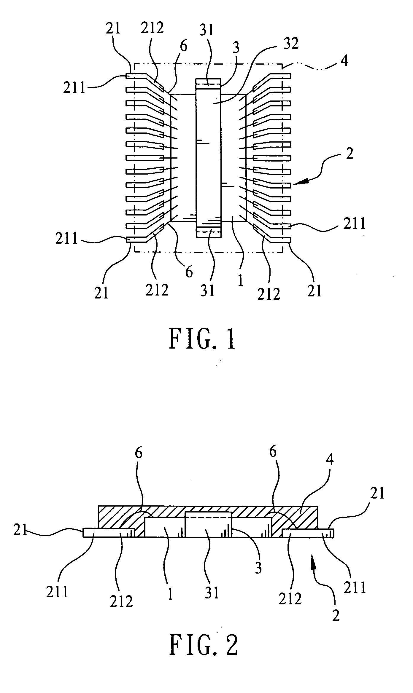
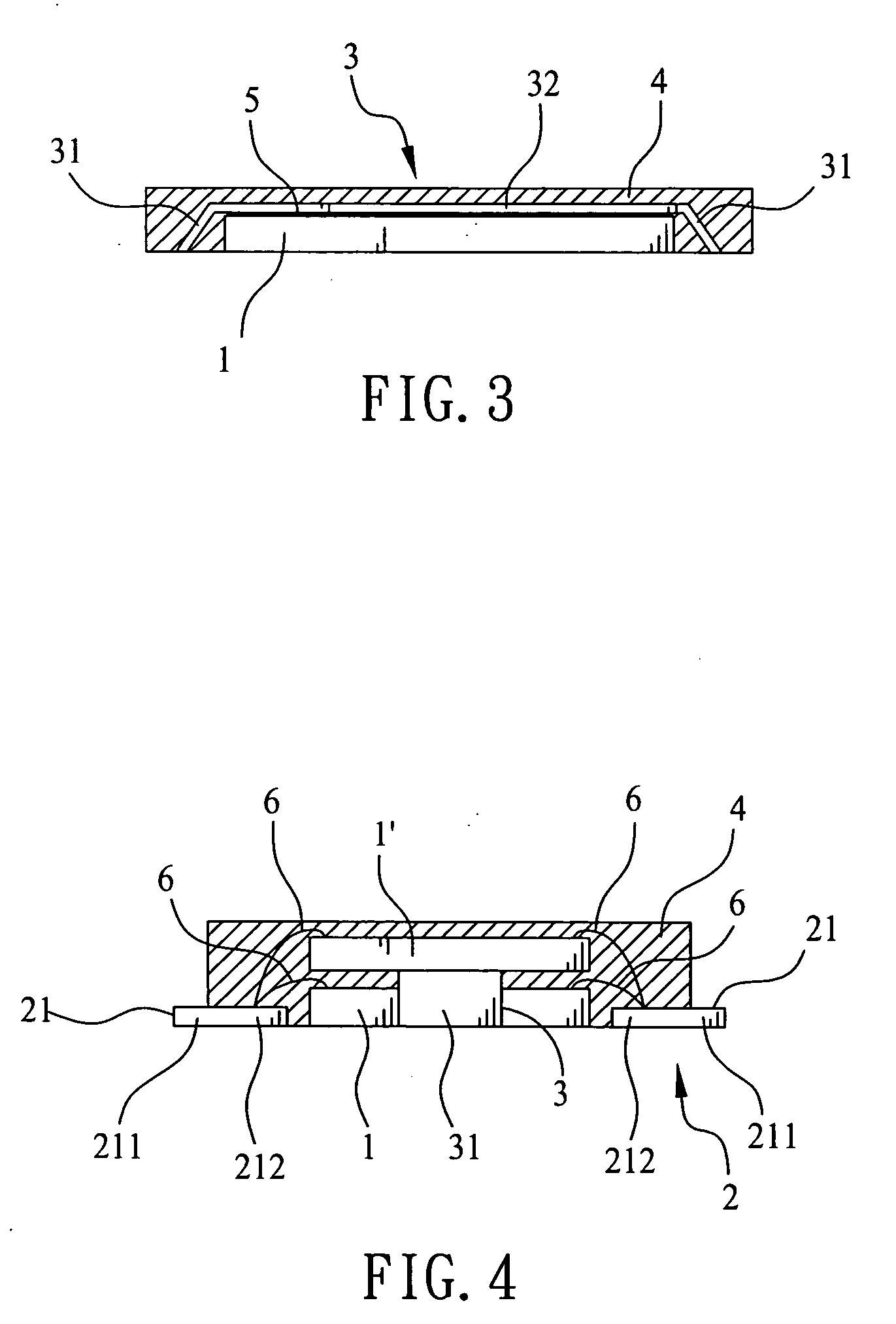
[0014] Please refer to FIG. 1 that is a top plan view showing the packaging structure of an IC with stably mounted chip according to a first embodiment of the present invention. As shown, the IC includes a chip 1, a leadframe 2, a bridge 3, and an encapsulating compound 4.

[0015] Please refer to FIGS. 1, 2, and 3 at the same time. The chip 1 is a product formed by known techniques and is therefore not described in details herein. The leadframe 2 includes a plurality of leads 21 arranged at two opposite lateral sides or all four sides of the leadframe 2 to electrically connect to external elements. Each of the leads 21 includes an outer and an inner electrical connecting end 211, 212. The encapsulating compound 4 is an insulating material covering the chip 1 and the inner electrical connecting ends 212 of the leadframe 2. The bridge 3 is a flat arch or an inverted U-shaped member made of a sheet material, and includes a supporting section 31 downward extended from each end of a horiz...


PUM


Abstract

An IC with stably mounted chip includes a chip, a leadframe, a bridge, and an encapsulating compound. The bridge is a flat arch made of a sheet material and includes a horizontal fixing section and a supporting section downward extended from each end of the fixing section. The chip is adhered to a bottom side of the fixing section of the bridge. The leadframe includes a plurality of leads arranged at two opposite sides of the chip. The encapsulating compound is applied to cover the chip, the bridge, and inner portions of the leads to complete a compact IC having a stably mounted chip and a reduced overall thickness. An additional chip may be adhered to a top of the bridge.

Description

FIELD OF THE INVENTION [0001] The present invention relates to an IC with stably mounted chip, and more particularly to an IC having a stably mounted chip and a reduced overall thickness, and allowing an additional chip to stack on the first chip. BACKGROUND OF THE INVENTION [0002] A conventional IC, as shown in FIG. 5, includes a chip 10 and a leadframe 20 located some distance lower than the chip 10. The leadframe 20 includes a plurality of leads 201 made of a sheet material and arranged at two opposite sides of the leadframe 20 for electrically connecting the chip 10 to external elements. The leads 201 are connected to contacts on the chip 10 via a metal wire 30, which may be a golden wire. The chip 10 is usually enclosed by an encapsulating compound 40 to complete the IC. In the above-described IC packaging structure, since the leads 201 are bent in configuration, the completed IC has an increased thickness that does not meet the compactness requirement of the current electronic...

Claims


Application Information

Patent Timeline
Patent Type & Authority Applications(United States)
IPC IPC(8): H01L23/02H01L23/495H01L23/16H01L23/28
CPCH01L23/16H01L23/49575H01L2224/48091H01L24/48H01L2224/48247H01L2924/00014H01L24/45H01L2224/451H01L2924/14H01L2924/181H01L2924/18165H01L2924/00015H01L2924/00H01L2924/00012
Inventor TZU, CHUNG-HSINGCHANG, SHIH-YI
Owner TZU CHUNG HSING
Why Eureka
Try Eureka