Method of dividing wafer

a technology of dividing wafers and wafers, applied in the direction of basic electric elements, semiconductor/solid-state device manufacturing, electric devices, etc., can solve the problems of denatured layer wafers along the streets being very susceptible to cracking, damaged or broken,

Active Publication Date: 2009-06-04
DISCO CORP
View PDF1 Cites 38 Cited by
  • Summary
  • Abstract
  • Description
  • Claims
  • Application Information

AI Technical Summary

Benefits of technology

[0008]Accordingly, it is an object of the present invention to provide a method of dividing a wafer by which a wafer provided therein with

Problems solved by technology

Meanwhile, the wafer provided therein with the denatured layer along the streets is very susceptible to cracking.
Therefore, the wafer may be broken or damaged in a feeding step in which the wafer provided therein with the denatured layer is fed from the laser beam mac

Method used


Image

  • Method of dividing wafer
  • Method of dividing wafer
  • Method of dividing wafer

Examples


Embodiment Construction

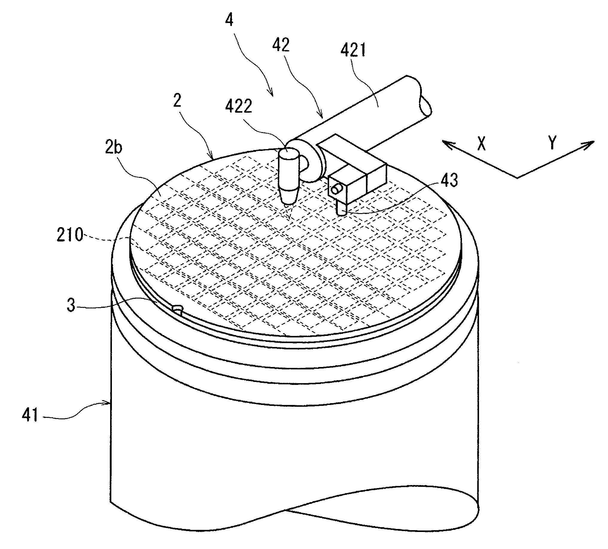
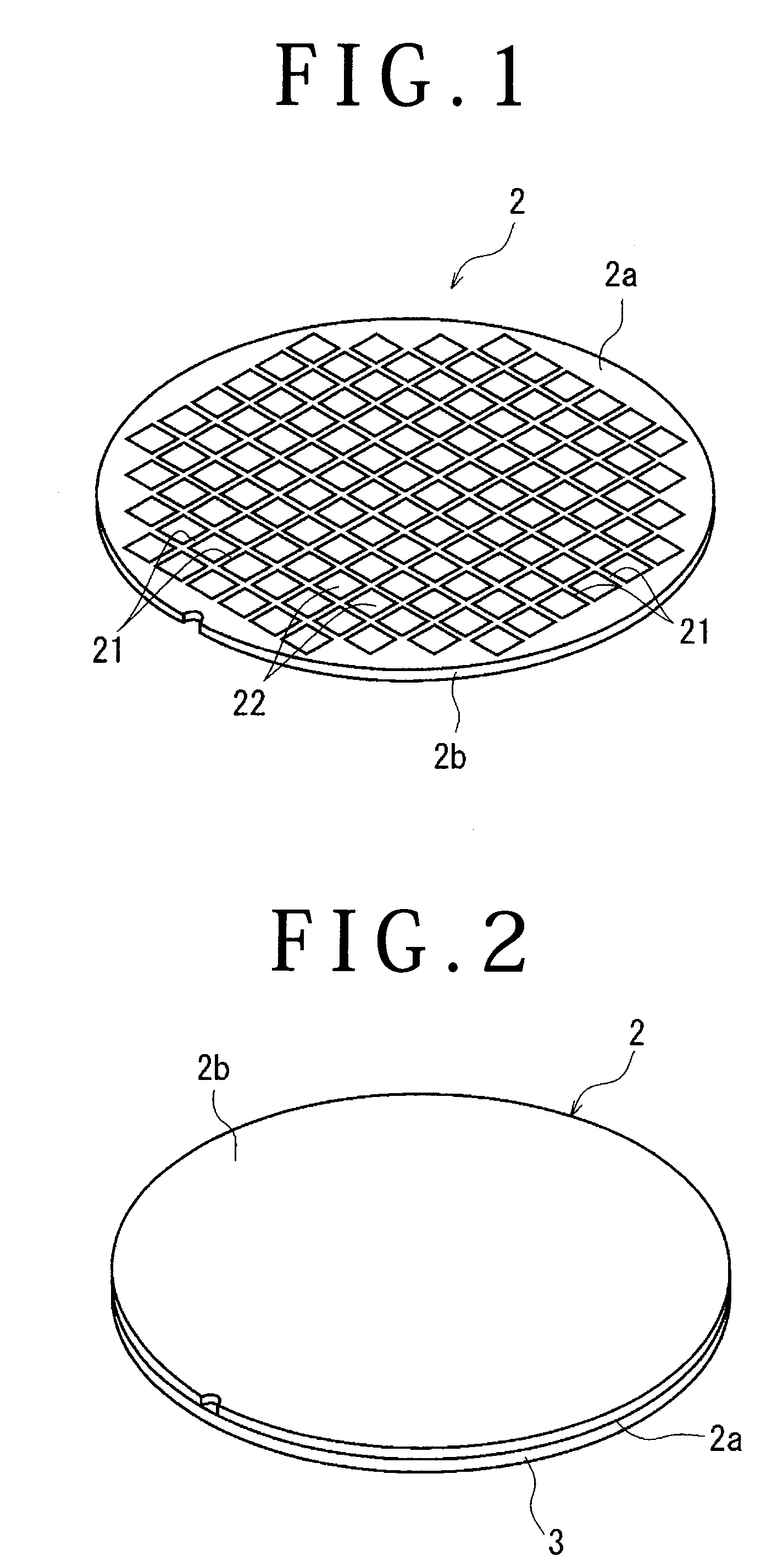
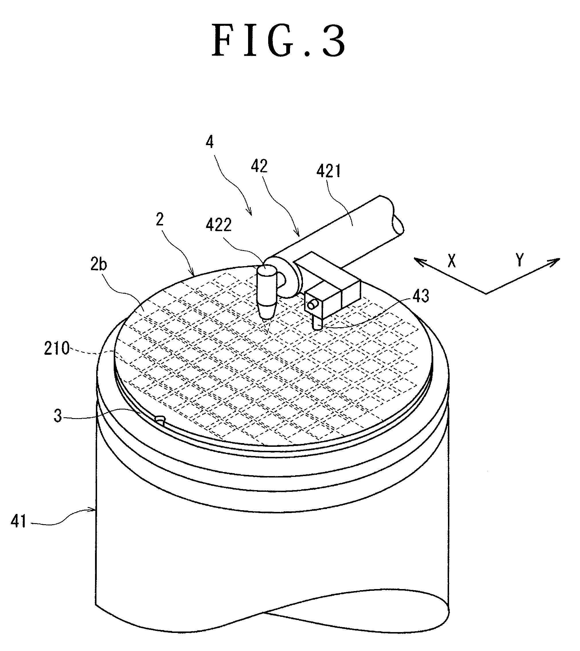
[0027]Now, a preferred embodiment of the method of dividing a wafer according to the present invention will be described in detail below, referring to the attached drawings. FIG. 1 shows a perspective view of a semiconductor wafer as a wafer to be divided by the method of dividing a wafer according to the present invention. The semiconductor wafer 2 shown in FIG. 1 is included of a silicon wafer having a thickness of 150 μm, for example, and is provided in its face-side surface 2a with a plurality of streets 21 in a grid pattern. At the face-side surface 2a of the semiconductor wafer 2, devices 22 such as ICs and LSIs are formed in a plurality of regions demarcated by the plurality of streets 21. Now, the method of dividing a wafer by which the semiconductor wafer 2 is divided into the individual devices 22 (chips) will be described below. In order to protect the devices 22, a protective tape 3 is adhered to the face-side surface 2a of the semiconductor wafer 2 as shown in FIG. 2 (p...


PUM


Abstract

A method of dividing a wafer includes: a denatured layer forming step of forming a denatured layer in the inside of the wafer along streets; a first feeding step in which the whole area of the wafer's back-side surface is suction held, and the wafer is mounted on a support base of a tape adhering unit, with the wafer's back-side surface on the upper side; a dicing tape adhering step of adhering a dicing tape to the wafer's back-side surface and an annular frame; a wafer reversing step of reversing the wafer and the annular frame face side back; a second feeding step of feeding said wafer and said annular frame to a tape expanding unit whole holding them by suction; a protective tape peeling step of peeling off a protective tape adhered to the wafer's face-side surface; and a wafer dividing step of expanding the dicing tape so as to divide the wafer along the streets along which the denatured layer has been formed.

Description

BACKGROUND OF THE INVENTION[0001]1. Field of the Invention[0002]The present invention relates to a method of dividing a wafer, provided in its face-side surface with a plurality of streets in a grid pattern and provided with devices in a plurality of regions demarcated by the plurality of streets, along the streets into the individual devices (chips).[0003]2. Description of the Related Art[0004]In the semiconductor device manufacturing process, usually, a plurality of regions are demarcated by planned dividing lines called streets arranged in a grid pattern in a surface of a substantially circular disk-shaped semiconductor wafer, and devices such as ICs and LSIs are formed in the thus demarcated regions. Then, the wafer is cut along the streets, to manufacture the individual devices. Similarly, an optical device wafer in which a gallium nitride compound semiconductor and the like are laminated on a surface of a sapphire substrate is also cut along streets, to be divided into individ...

Claims


Application Information

Patent Timeline
IPC IPC(8): H01L21/302
CPCH01L21/78H01L21/67132
Inventor NAKAMURA, MASARU
Owner DISCO CORP
Why Eureka
Try Eureka