Method of cutting adhesive film on a singulated wafer backside

a technology of adhesive film and backside, which is applied in the direction of welding/soldering/cutting articles, electrical equipment, laser beam welding apparatus, etc., can solve the problems of affecting the quality of adhesive film, so as to prevent the damage to the chip and the electrical problems caused by the back surface of the chip. , the effect of high quality

Inactive Publication Date: 2009-12-03
DISCO CORP
View PDF3 Cites 32 Cited by
  • Summary
  • Abstract
  • Description
  • Claims
  • Application Information

AI Technical Summary

Benefits of technology

[0010]With the device of the present invention, the entire back surface of the chip is protected by the adhesive film. Therefore, even if mold resin is filled in a periphery of the device, filler included in the mold resin does not enter the back surface of the chip, thereby avoiding problems such as damage to the chip by the filler. If the devices of the invention are stacked, the back surface of the chip is prevented from coming into contact with a bonding wire of the device on the stacked side because the adhesive film is interposed. Therefore, electrical problems such as short circuiting and leakage are prevented.
[0015]With the present invention, it is possible to obtain a device in which the entire back surface of a chip is reliably covered with an adhesive film. Therefore, it is possible to provide a device of high quality in which damage to the chip and electrical problems caused by exposure of a part of the back surface of the chip are prevented.

Problems solved by technology

However, if the adhesive film does not cover the entire back surface of the semiconductor chip, and if a small part of an edge of the back surface is exposed, for example, a filler material included in the mold resin and called “filler” (with a particle diameter of about 10 to 20 μm and including silica, for example) may damage the exposed face on which the adhesive film is not adhered or may be pushed into a small gap between the exposed face and the stacked object, thereby causing cracking or chipping of the semiconductor chips.
Especially in the extremely thin semiconductor chips having thicknesses of 100 μm or less, such a problem is likely to occur.
In this case, if the back surface includes the exposed face which is not covered with the adhesive film as described above, the exposed portion may come into contact with a bonding wire of the semiconductor chip on the stacked object side, thereby causing electrical problems such as short circuiting and leakage.

Method used


Image

  • Method of cutting adhesive film on a singulated wafer backside
  • Method of cutting adhesive film on a singulated wafer backside
  • Method of cutting adhesive film on a singulated wafer backside

Examples


first embodiment

1. Manufacturing Method for the First Embodiment

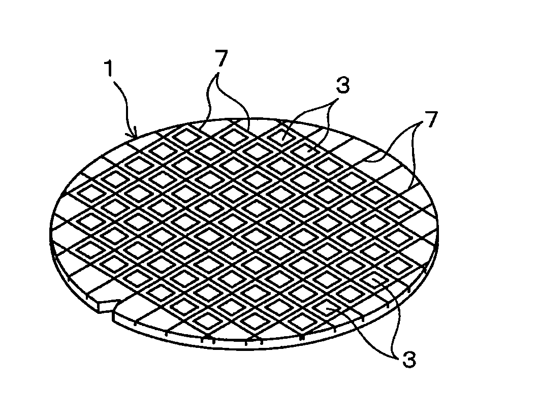
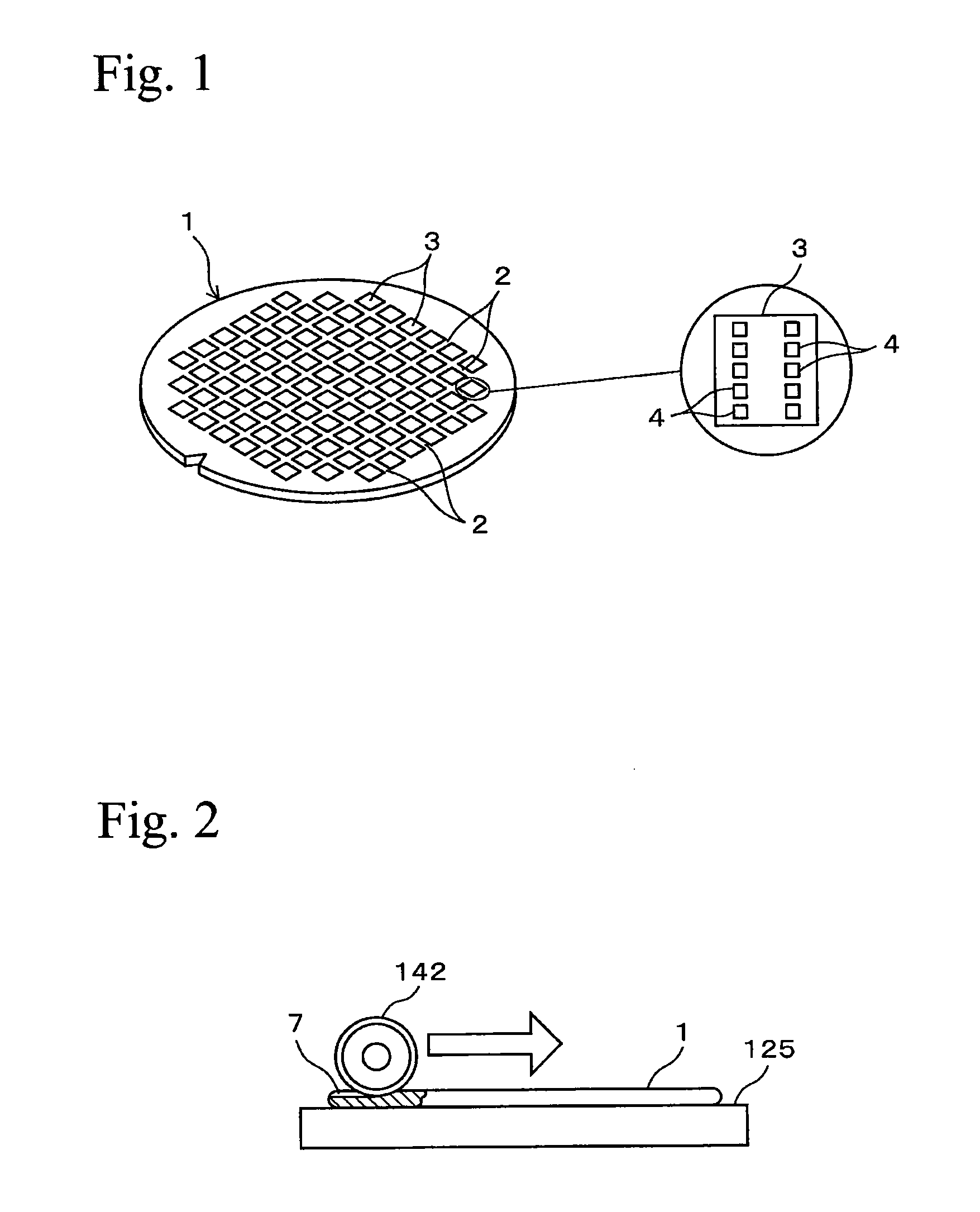
[0031]A reference numeral 1 in FIG. 1 designates a disk-shaped semiconductor wafer formed of a silicon wafer or the like. As shown in FIG. 1, on a front surface of the wafer 1, rectangular chip regions 3 are defined by lattice-shaped streets (predetermined division lines) 2. On a front surface of each of these chip regions 3, electronic circuits (functional elements) 4 are formed as shown in an enlarged portion in FIG. 1.

[0032]The chip regions 3 are separated from each other by the manufacturing method of the present embodiment, and each of the regions becomes a chip 6 of a semiconductor chip (device) 5 with an adhesive film and which will be described later (see FIG. 9). A thickness of the wafer 1 is greater than a thickness of the chip 6 to be produced. The embodiment is a method for manufacturing the semiconductor chip with a two-layered structure in which an adhesive film such as a DAF is adhered on a back surface of the chip 6; th...

second embodiment

2. Manufacturing Method for the Second Embodiment

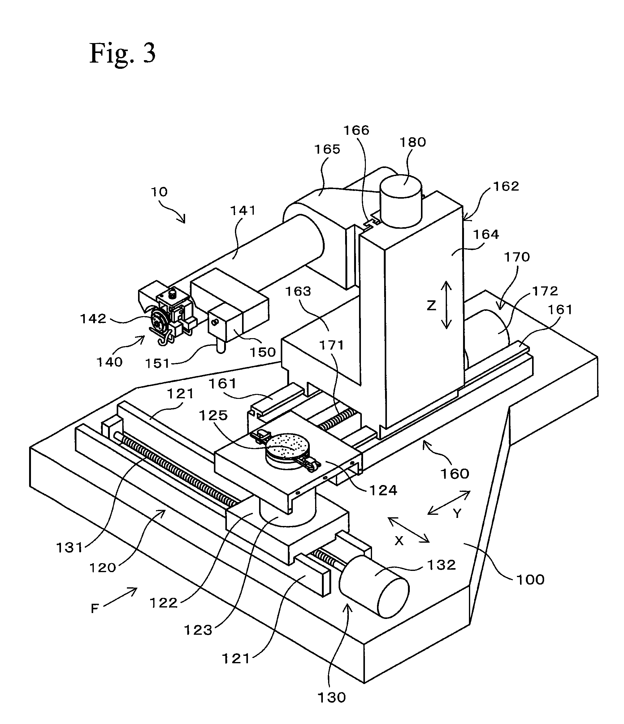
[0068]Next, a manufacturing method for a second embodiment of the invention will be described. This manufacturing method is the same as that of the first embodiment up until the adhesive film adhering step and differs in the adhesive film cutting step after the adhesive film adhering step. In the adhesive film cutting step in the second embodiment, as shown in FIG. 10, a laser beam is applied to the adhesive film 9 through the division grooves 7 from a laser beam irradiation device 60 to thereby cut the adhesive film 9 along the division grooves 7. In this way, the semiconductor chip 5 in which the adhesive film 9 is adhered on the back surface of the chip 6 is obtained. In order to apply the laser beam to the adhesive film 9 along the division grooves 7, the laser beam irradiation device 60 is mounted in place of the cutting blade 142 of the dicing device 10 shown in FIG. 3 and the aligner 150 controls the location at which the laser...

third embodiment

3. Manufacturing Method for the Third Embodiment

[0069]Next, a manufacturing method for a third embodiment of the invention will be described.

(1) Back Surface Grinding Step

[0070]First, the back surface of the wafer 1 shown in FIG. 1 is ground until the wafer 1 becomes as thin as the chip 6 to be obtained. For this purpose, as shown in FIG. 11, the wafer 1 on the front surface of which the protection film 8 has been adhered is suctioned and held on the chuck table 317 of the grinding device 30 shown in FIG. 7 with the back surface of the wafer 1 facing up and the back surface is ground with the grindstones 326 of the grinding wheel 327.

(2) Inside Modified Layer Forming Step

[0071]Then, the laser beam is applied to the insides of the streets 2 of the wafer 1 along the streets 2 to change the portion to which the laser beam is applied into the inside modified layer. This inside modified layer is a layer that has been melted and set again so that the layer is reduced in strength. The laye...


PUM

PropertyMeasurementUnit
particle diameteraaaaaaaaaa
thicknessesaaaaaaaaaa
Tgaaaaaaaaaa

Abstract

On the back surface of the chip of which a front surface is formed with an electronic circuit, an adhesive film of a shape and dimensions corresponding to at least the back surface of the chip is adhered to obtain the semiconductor chip with the entire back surface covered with the adhesive film. Such a semiconductor chip is obtained by forming a division groove in the front surface of a semiconductor wafer to be divided into plural chips, grinding a back surface of the wafer until the division groove appears to divide the wafer into plural chips, adhering the adhesive film and a dicing tape on the entire back surface of the wafer, and stretching the dicing tape to cut the adhesive film along the division groove.

Description

RELATED APPLICATIONS[0001]This application is a Division of U.S. patent application Ser. No. 11 / 519,321 filed on Sep. 12, 2006, which claims priority to Japanese Patent Application No. JP2005-265477 filed on Sep. 13, 2005, the entire contents of which are herein incorporated by reference.BACKGROUND OF THE INVENTION[0002]1. Field of the Invention[0003]The present invention relates to a technique relating to a device such as a semiconductor chip, and in particular, relates to a device on a back surface of which an adhesive film is adhered, and to a manufacturing method for the device.[0004]2. Related Art[0005]In recent techniques for semiconductor devices, a stacked package such as an MCP (Multi-Chip Package) and a SiP (System in Package), in which a plurality of semiconductor chips are stacked, is used effectively in order to achieve high density and miniaturization. On a back surface of the semiconductor chip provided in such a technique, an adhesive film called a DAF (Die Attach Fi...

Claims


Application Information

Patent Timeline
Patent Type & Authority Applications(United States)
IPC IPC(8): H01L21/304
CPCB23K26/0054B23K26/4075B23K26/0057H01L24/29H01L2924/0665H01L2924/01033H01L2924/01006H01L2224/2919H01L21/6835H01L21/6836H01L21/78H01L24/27H01L24/83H01L2221/68327H01L2221/68336H01L2221/6834H01L2224/274H01L2224/83191H01L2224/8385H01L2924/01005H01L2924/01075H01L2924/01082H01L2924/07802H01L2924/00H01L2924/3512B23K26/40B23K26/50B23K26/53B23K2103/50H01L2924/181
Inventor ARAI, KAZUHISANAKAMURA, MASARU
Owner DISCO CORP
Why Eureka
Try Eureka