

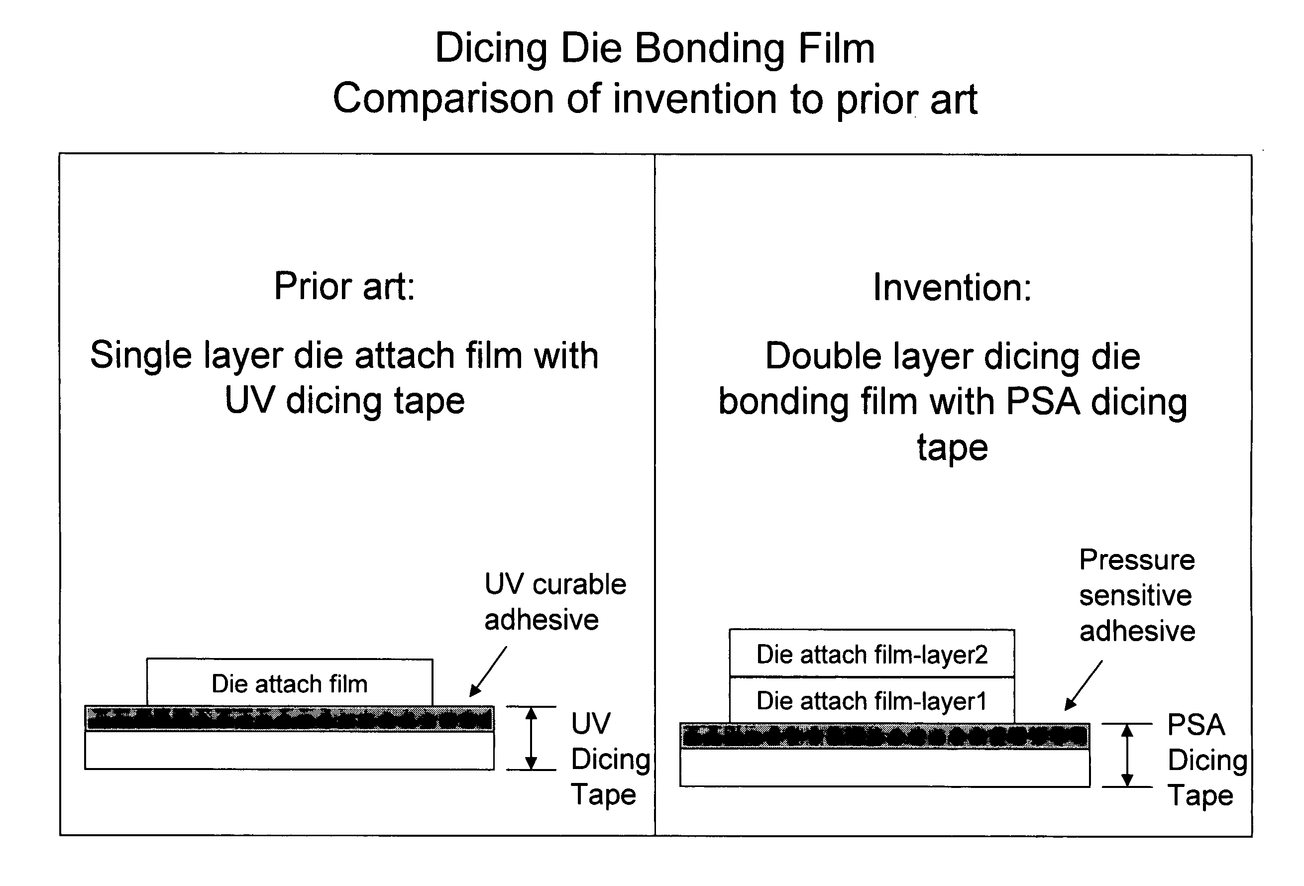
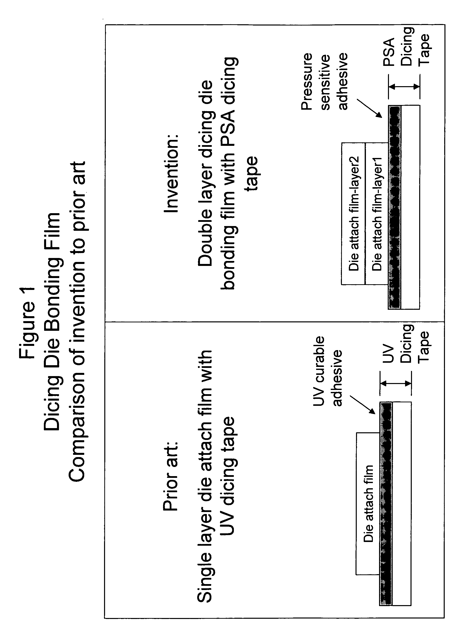
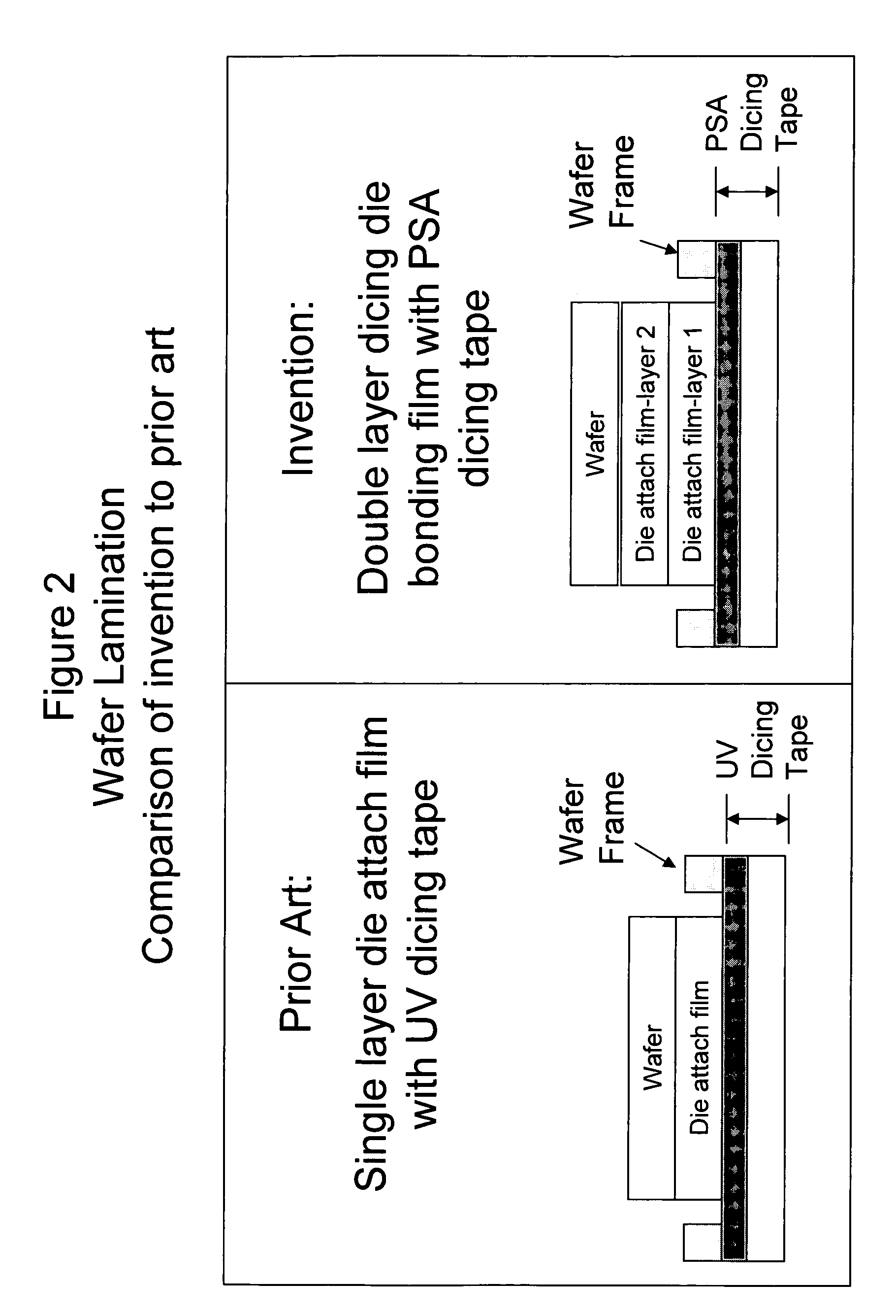
Dicing die bonding film
a bonding film and die technology, applied in the direction of film/foil adhesives without carriers, film/foil adhesives, transportation and packaging, etc., can solve the problems of significant deformation of wafers, inadequate adhesion to silicon dies, and pull away
- Summary
- Abstract
- Description
- Claims
- Application Information
AI Technical Summary
Benefits of technology
Problems solved by technology
Method used
Image

Examples
example 1
Film A
[0029] Layer 1 (for adhesion to a dicing tape) was prepared by mixing the following components in parts by weight (pbw) in sufficient methyl ethyl ketone to make a paste:
[0030] 60 pbw epoxy-modified CTBN (Mn: 15015, Tg: −17° C.);
[0031] 29 pbw cresol novolac epoxy (epoxy equivalent: 220, softening point: 90° C.);
[0032] 7 pbw 3,3′diaminodiphenyl sulfone,
[0033] 1 pbw 2-phenyl 4-methyl imidazol
[0034] 3 pbw silica filler (average size : 0.5 μm)
This paste was coated onto a 50 μm thick release-coated polyester film and dried at 90° C. for 5 minutes to make Film A, Layer 1 at 10 μm thickness.
[0035] Layer 2 for adhesion to a silicon wafer was prepared by mixing the following components in parts by weight (pbw) in sufficient methyl ethyl ketone to make a paste:
[0036] 60 pbw epoxy-modified CTBN (Mn: 15015, Tg: −17° C.),
[0037] 30 pbw bisphenol F epoxy( epoxy equivalent: 290, softening point: 4° C., viscosity: 35,000 mPaS at 50° C.),
[0038] 6 pbw 3,3′diaminodiphenyl sulfone,
[00...
example 2
Film B
[0043] Layer 1 (for adhesion to a dicing tape) was prepared by mixing the following components in parts by weight (pbw) in sufficient methyl ethyl ketone to make a paste:
[0044] 60 pbw epoxy-modified CTBN (Mn: 15015, Tg: −17° C.), 29 pbw cresol novolac epoxy (epoxy equivalent: 220, softening point: 90° C.),
[0045] 7 pbw 3,3′diaminodiphenyl sulfone,
[0046] 1 pbw 2-phenyl 4-methyl imidazol
[0047] 3 pbw silica filler (average size: 0.51 μm)
[0048] This paste was coated onto 50 μm thick release-coated polyester film and dried at 90° C. for 5 minutes to make Layer 1 at 13 μm thickness.
[0049] Layer 2 for adhesion to a silicon wafer was prepared by mixing the following components in parts by weight (pbw) in sufficient methyl ethyl ketone to make a paste:
[0050] 25 pbw carboxylated acrylonitrile butadiene copolymer rubber (Mw: 350,000, acrylonitrile content: 27 wt %, Tg: −20° C.),
[0051] 15 pbw vinyl terminated butadiene-nitrile rubber (acrylonitrile content: 21.5%, Tg: −45° C.),
[0...
example 5
Performance and Test Method
[0072] Each of the Films A to D and a commercially available single layer ve tape (Film H) was laminated to a silicon wafer at various atures, and tested for 90° peel strength. The results of this testing are in Table 1.
TABLE 1Peel Strength at Various Lamination Temperatures (N / cm)Lamin.Temp.(° C.)SubstrateFilm AFilm BFilm CFilm DFilm H30Dicing Tape0.140.130.150.5930Silicon Wafer0.750.530.020.6940Dicing Tape0.150.150.160.650.1040Silicon Wafer0.850.670.030.680.0850Dicing Tape0.160.170.190.770.0850Silicon Wafer0.830.740.050.670.1360Dicing Tape0.180.190.180.80.0760Silicon Wafer0.910.850.270.840.1670Dicing Tape0.210.230.190.840.0870Silicon Wafer0.950.830.520.960.3580Dicing Tape0.250.260.230.970.0680Silicon Wafer1.10.880.680.920.5190Dicing Tape0.240.230.251.0290Silicon Wafer1.150.910.820.96
[0073] Results indicate that both multi-layer Films A and B give acceptable peel strengths for good dicing and die pick up performance of between 0.05 and less than 0.5 N / ...
PUM
| Property | Measurement | Unit |
|---|---|---|
| Temperature | aaaaa | aaaaa |
| Fraction | aaaaa | aaaaa |
| Percent by mass | aaaaa | aaaaa |
Abstract
Description
Claims
Application Information