Wafer dividing method

a dividing method and wafer technology, applied in the field of wafer dividing method, can solve the problems of difficult laser beam focus adjustment, wafer may crack along the modifying layer, and warp at the outer circumference, and achieve the effect of small thickness

Inactive Publication Date: 2008-11-13
DISCO CORP
View PDF8 Cites 30 Cited by
  • Summary
  • Abstract
  • Description
  • Claims
  • Application Information

AI Technical Summary

Benefits of technology

[0007]Accordingly, it is an object of the present invention to provide a wafer dividing method that can surely form a modifying layer al

Problems solved by technology

However, if a wafer is formed to have a thickness of 100 μm or less, it will causes warps at the outer circumference thereof.
This makes it difficult to adjust the f

Method used


Image

  • Wafer dividing method
  • Wafer dividing method
  • Wafer dividing method

Examples


first embodiment

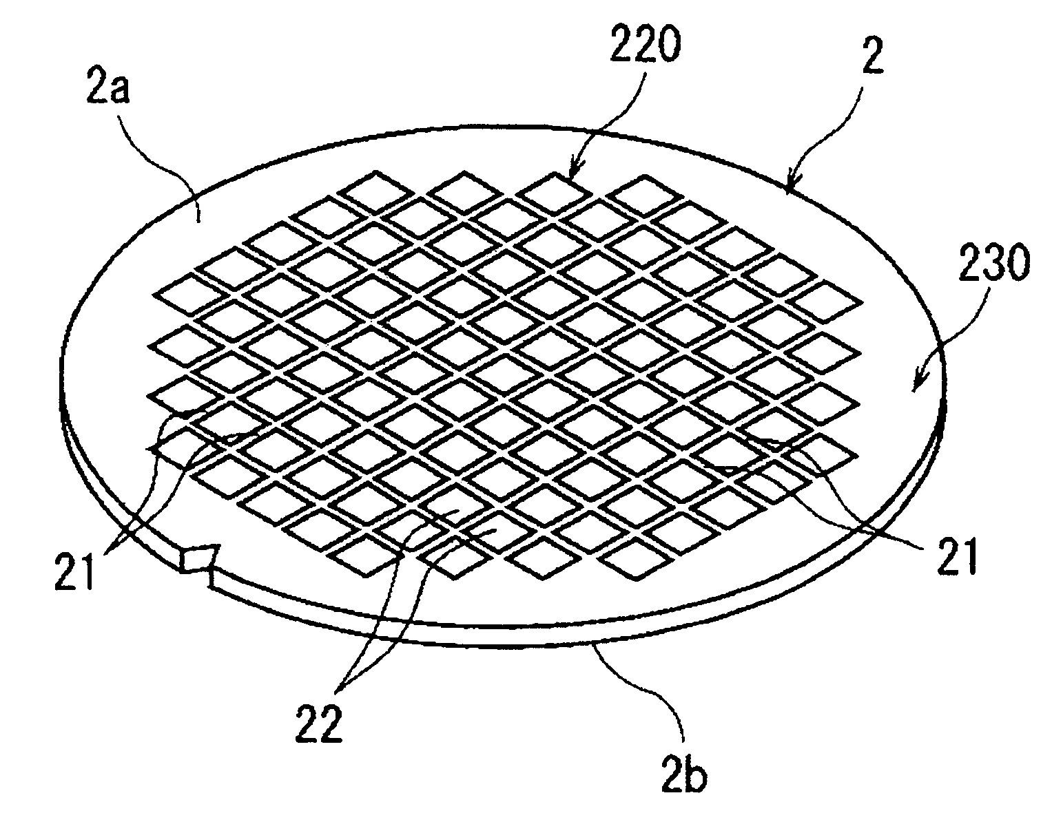
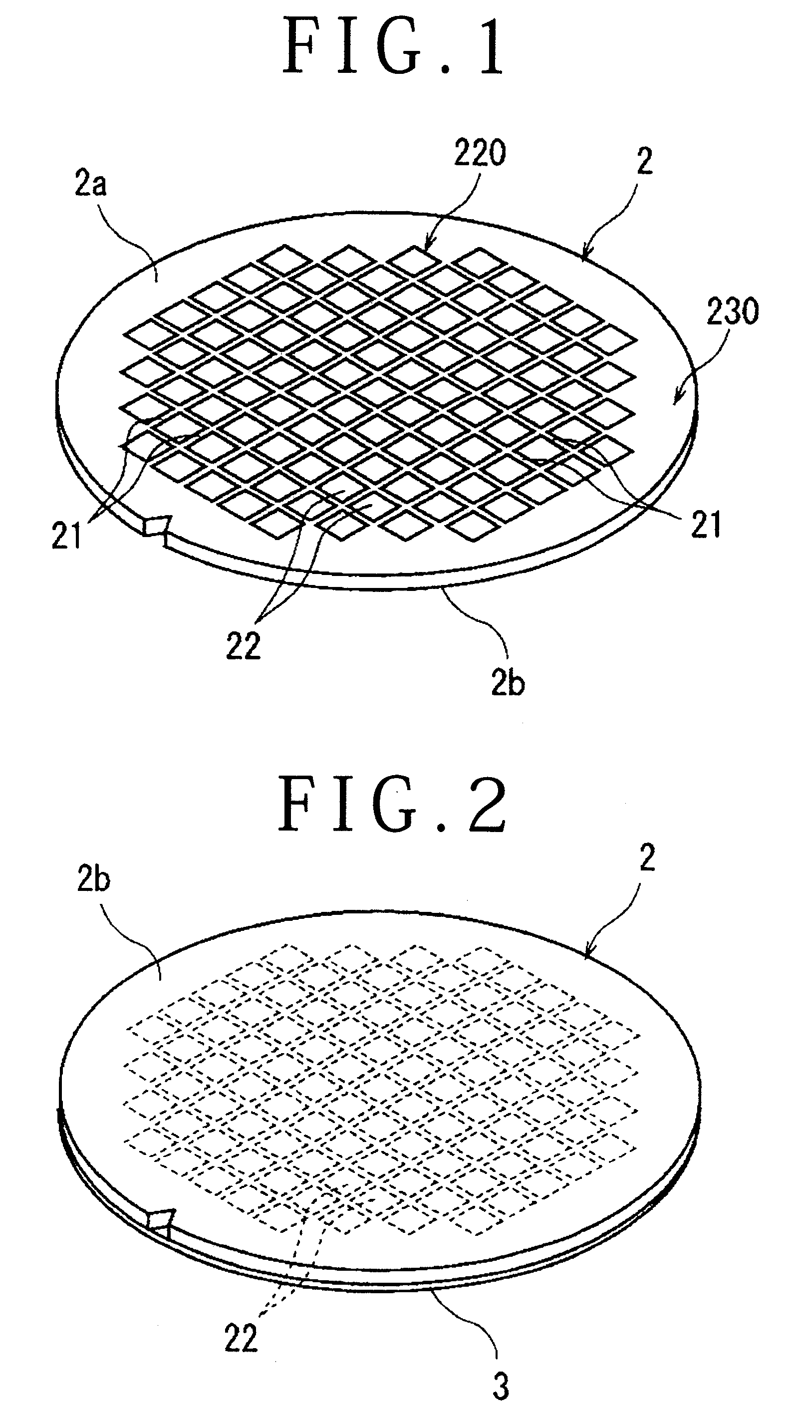
[0029]A first embodiment in which the semiconductor wafer 2 is divided along the streets 21 into the individual devices is described with reference to FIGS. 2 through 13B. When the semiconductor wafer 2 is divided along the streets 21 into the individual devices, a protection member 3 is stuck to the front surface 2a of the semiconductor wafer 2 as shown in FIG. 2 (a protection member sticking step). Thus, the rear surface 2b of the semiconductor wafer 2 is exposed.

[0030]After the execution of the protection member sticking step, a modifying layer forming step is performed. In this step, a laser beam with a wavelength that can pass through the semiconductor wafer 2 is focused on the inside of the semiconductor wafer 2 from the rear surface 2b thereof and applied thereto along the street 21. This application forms a modifying layer having a thickness from the front surface 2a of the semiconductor wafer 2 corresponding to at least the finishing thickness of the device 22. This modifyi...

second embodiment

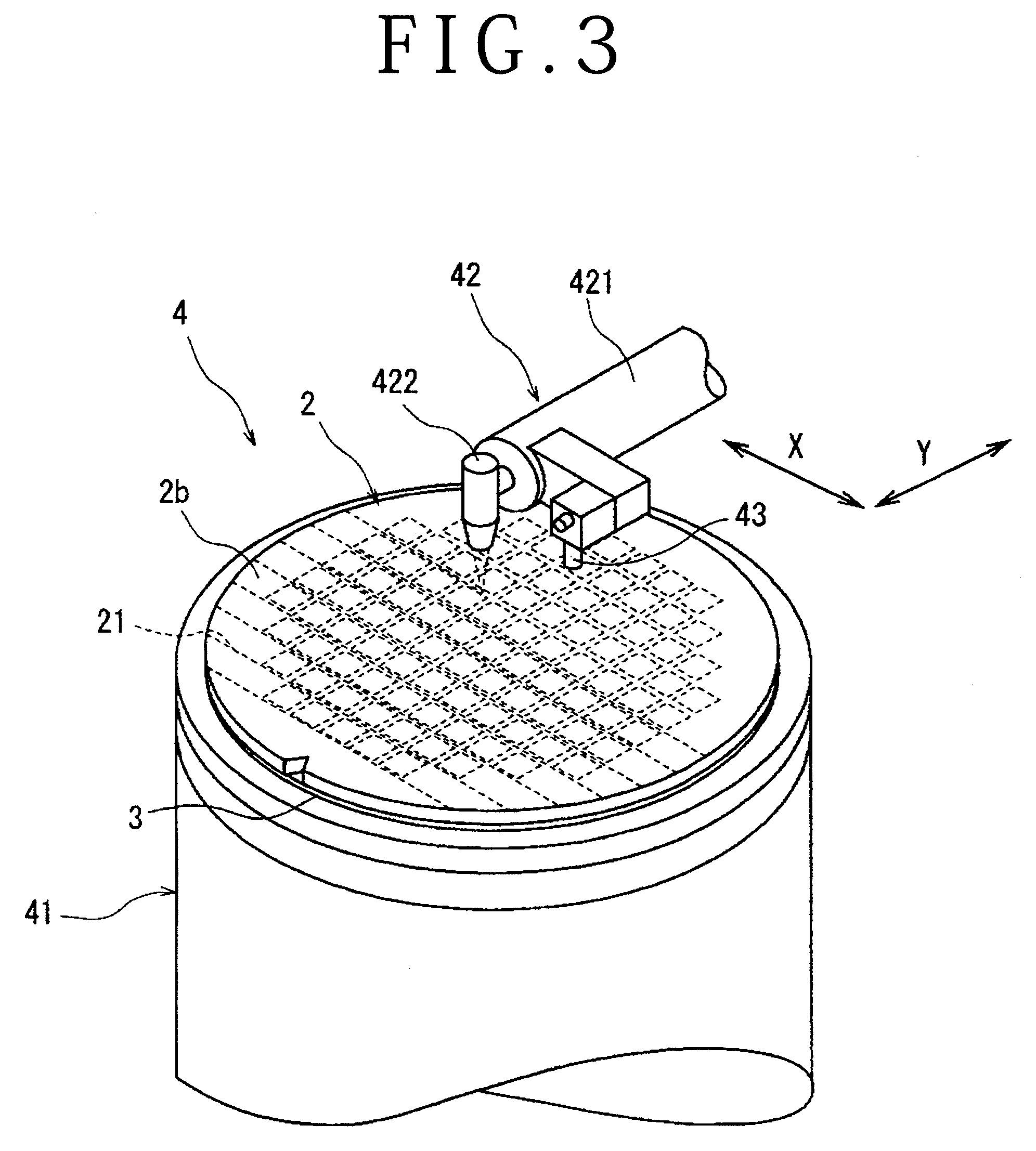
[0058]In this case, it is enough that a laser beam irradiation range is the device area 220 of the semiconductor wafer 2, that is, a laser beam is not applied to the outer circumferential redundant area 230 formed with the annular reinforcing section 230b. As described above, the modifying layer forming step in the second embodiment is executed after the portion of the rear surface of the semiconductor wafer 2 corresponding to the device area 220 is ground and formed to have the finishing thickness (e.g. 50 μm) of the device 22. However, the annular reinforcing section 230b is formed at the area of the semiconductor wafer 2 corresponding to the outer circumferential redundant area surrounding the device area 220. Thus, the semiconductor wafer 2 causes no warps at the outer circumference thereof. Consequently, the modifying layer forming step can surely form the modifying layers 210 at respective predetermined internal positions of the semiconductor wafer 2 so as to extend along the ...


PUM


Abstract

A wafer dividing method that includes a modifying layer forming step in which a laser beam with a wavelength that can pass through the wafer is focused on the inside of the wafer from a rear surface side thereof, and applied along the street to form a modifying layer having a thickness corresponding to at least a device-finishing thickness from the front surface of the wafer; a rear surface grinding step in which an area, corresponding to the device area, of the rear surface of the wafer subjected to the modifying layer forming step is ground and formed to have a thickness corresponding to the device-finishing thickness and to have an annular reinforcing section at an area corresponding to the outer circumferential redundant area; a reinforcing section cutting step in which the wafer is cut along the inner circumference of the annular reinforcing section; a wafer support step in which the rear surface of the wafer whose annular reinforcing section is cut is stuck to a dicing tape attached to an annular frame; and a wafer rupture step in which an external force is applied to the wafer stuck to the dicing tape to rupture it along the street formed with the modifying layer.

Description

BACKGROUND OF THE INVENTION[0001]1. Field of the Invention[0002]The present invention relates to a method of dividing a wafer along a plurality of streets arranged in a lattice pattern on the front surface of the wafer, the wafer having a device area where devices are formed on a plurality of area sectioned by the streets and an outer circumferential redundant area surrounding the device area.[0003]2. Description of the Related Art[0004]In a semiconductor device fabrication process, the front surface of an almost-disklike semiconductor wafer is sectioned into a plurality of areas by predetermined dividing lines called streets arranged in a lattice pattern. Devices such as ICs, LSIs or the like are formed in the areas thus sectioned. The semiconductor wafer is cut along the streets to divide the areas formed with the devices therein for fabricating the individual devices. An optical device wafer in which gallium nitride-system compound semiconductor and the like are stacked on the fr...

Claims


Application Information

Patent Timeline
IPC IPC(8): H01L21/304B23K26/00B23K26/364
CPCB23K26/0057B23K26/4075B24B7/228B28D5/0011H01L21/6835H01L21/6836H01L21/78H01L2221/68327H01L2221/6834B23K26/40B23K26/53B23K2103/50
Inventor NAKAMURA, MASARU
Owner DISCO CORP
Why Eureka
Try Eureka