

Multi-function tape for a semiconductor package and method of manufacturing a semiconductor device using the same
a technology of multi-functional tapes and semiconductor devices, which is applied in the direction of heat-activated film/foil adhesives, film/foil adhesives, transportation and packaging, etc., can solve the problem of providing unnecessary space, and achieve the effect of increasing separation
- Summary
- Abstract
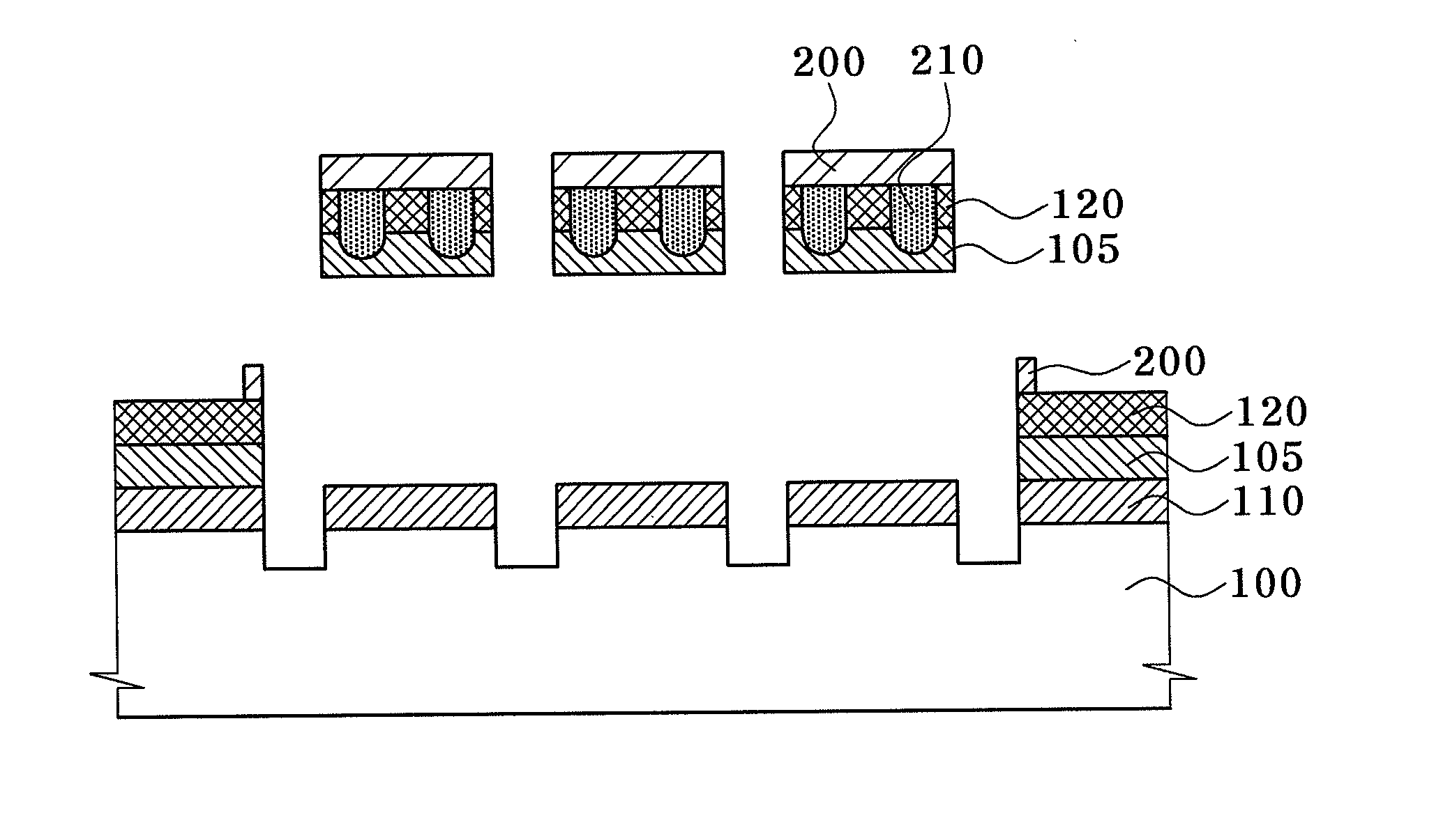
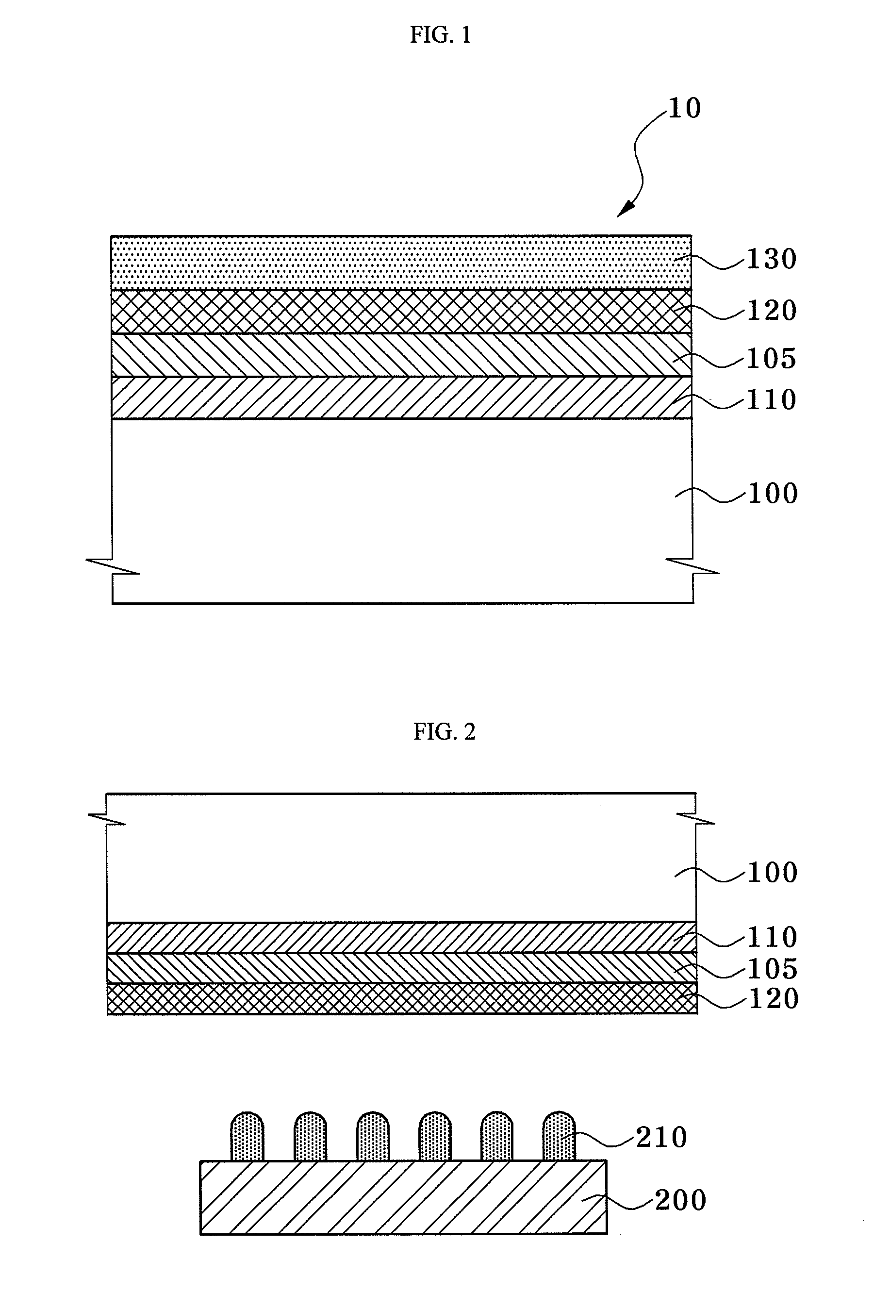
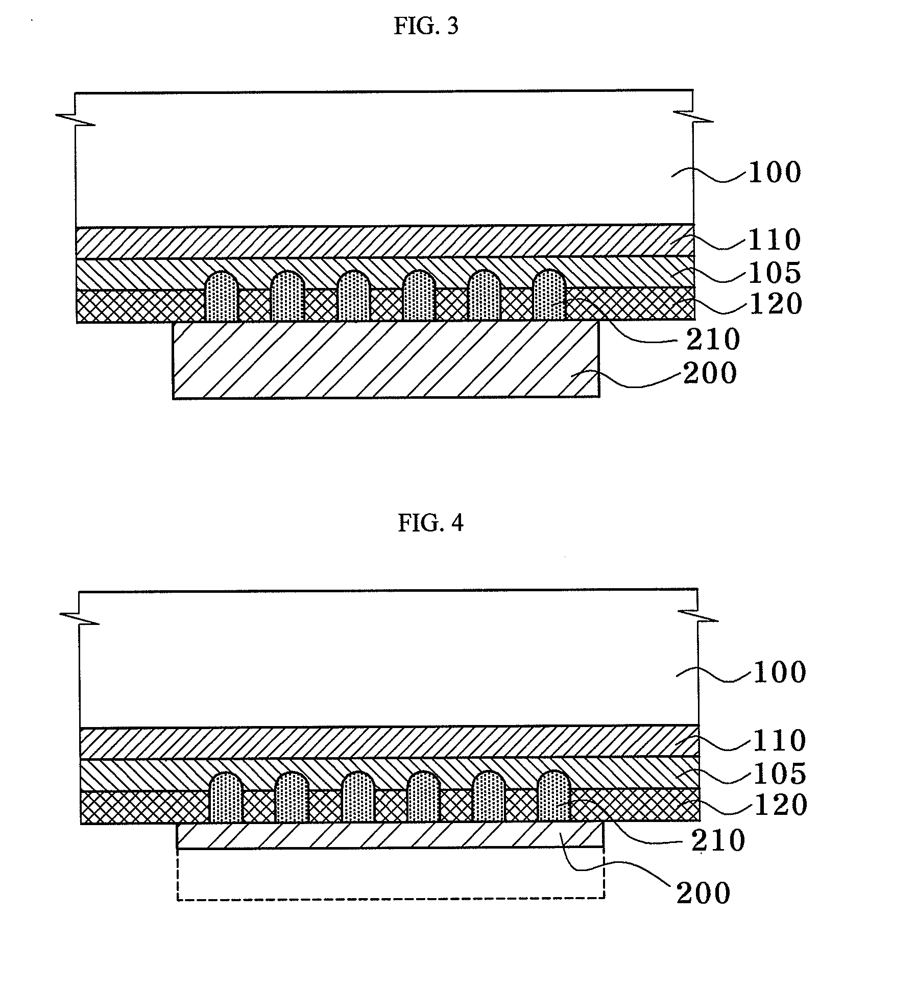
- Description
- Claims
- Application Information
AI Technical Summary
Benefits of technology
Problems solved by technology
Method used
Image

Examples
example 1
Preparation of an Adhesive Layer A-1
[0153]A reflux condenser, a thermometer, and a dropping funnel were equipped to a 2 L 4-neck flask in which 220 g of ethyl acetate and 150 g of toluene were charged.
[0154]After raising the temperature of the solution in the flask to 60° C., a mixture of methylmethacrylate 118 g, butylacrylate monomer 75 g, 2-ethylhexyl acetate 187 g, 2-hydroxyethylmethacrylate 120 g, acrylic acid 30 g, and benzoyl peroxide 2.0 g was added to the flask dropwise through the dropping funnel at 90° C. for 3 hours.
[0155]While adding the mixture, the solution was stirred at 250 rpm; and the reactant was then reacted for 3 hours at the same temperature. Then, 1.0 g of diazoisobutyronitrile was further added to the reactant in the flask, which in turn was maintained for 5 hours, thereby finishing polymerization.
[0156]Next, 15 g of isocyanoethylmethacrylate was added to the prepared polymer binder resin and reacted therewith at room temperature for 24 hours, thereby prepar...
PUM
| Property | Measurement | Unit |
|---|---|---|
| storage modulus | aaaaa | aaaaa |
| thickness | aaaaa | aaaaa |
| thickness | aaaaa | aaaaa |
Abstract
Description
Claims
Application Information