Method and apparatus for processing the image of the surface of a wafer recorded by at least one camera
- Summary
- Abstract
- Description
- Claims
- Application Information
AI Technical Summary
Benefits of technology
Problems solved by technology
Method used
Image

Examples
Embodiment Construction
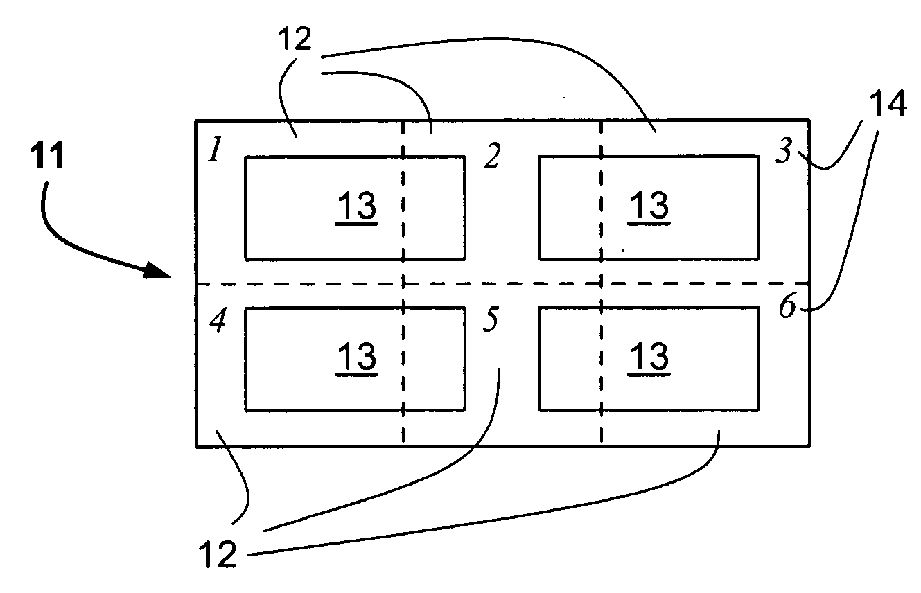
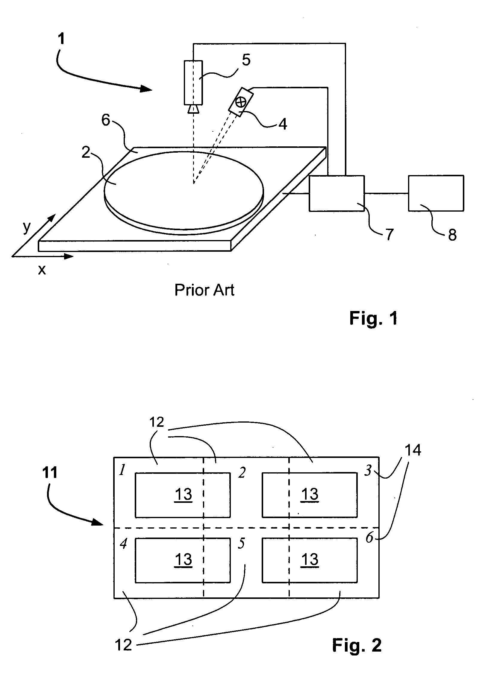
[0052]FIG. 1 schematically shows an apparatus 1 for processing image data of the surface of a wafer 2 recorded by a camera 5 according to the prior art. Wafer 2 is on a scanning stage 6. A plurality of images is taken of wafer 2 by means of camera 5. To create a relative movement between scanning stage 6 and camera 5, in the present exemplary embodiment, an X / Y scanning stage is used traversable in the X coordinate direction and / or the Y coordinate direction. Camera 5 is fixed with respect to scanning stage 6. Of course, scanning stage 6 can also be fixed, and camera 5 can be moved across wafer 2 for imaging. A combination of the movement of camera 5 in one direction and scanning stage 6 in the direction perpendicular thereto is also possible. Devices such as motors for moving the scanning stage and the camera can be provided.
[0053]Wafer 2 is illuminated by means of an illumination means or illuminator 4, which illuminates at least those areas on wafer 2 which essentially correspond...
PUM
 Abstract
Description
Claims
Application Information
 - Generate Ideas
- Intellectual Property
- Life Sciences
- Materials
- Tech Scout
- Unparalleled Data Quality
- Higher Quality Content
- 60% Fewer Hallucinations
Browse by: Latest US Patents, China's latest patents, Technical Efficacy Thesaurus, Application Domain, Technology Topic, Popular Technical Reports.
© 2025 PatSnap. All rights reserved.Legal|Privacy policy|Modern Slavery Act Transparency Statement|Sitemap|About US| Contact US: help@patsnap.com