Liquid Crystal Display Device

a liquid crystal display and display device technology, applied in non-linear optics, instruments, optics, etc., can solve the problems of lowering the open area ratio, light scattering, contrast reduction, etc., and achieve the reduction of the amount of liquid crystal used, the effect of fine control of the height of the spacer and the reduction of the cost of the materials for the liquid crystal display devi

Active Publication Date: 2009-06-18
PANASONIC LIQUID CRYSTAL DISPLAY CO LTD
View PDF24 Cites 19 Cited by
  • Summary
  • Abstract
  • Description
  • Claims
  • Application Information

AI Technical Summary

Benefits of technology

[0033]According to the present invention, spacers are formed by layering a number of color filters, and therefore a separate photolithographic process for forming spacers is not necessary, and in addition, the height of the spacers can be finely controlled by changing the area of the color filters which form the spacers.
[0034]In addition, according to the present invention, when first spacers and second spacers having different heights are formed, the area of the color filters for forming the first spacers and the second spacers varies, or the order of layering of the color filters varies so that the difference in the height between the first spacers and the second spacers is created, and thus the heights of the first spacers and the second spacers can be finely controlled.
[0035]Furthermore, according to the present invention, color filters are provided between pixels which do not contribute to the formation of an image, and therefore the amount of liquid crystal used can be reduced, and the cost of the materials for the liquid crystal display device can be reduced.

Problems solved by technology

When beads are dispersed, however, beads are also provided in regions where pixel electrodes are formed, and such a problem arises that light is scattered in these portions and the contrast lowers.
In addition, beads are dispersed into regions with pixels through which light from the backlight transmits, and this may cause a lowering of the open area ratio.
Meanwhile, in the case where multilayer support pillars are formed of color filters, color filters for each color must be precisely positioned in the support pillar portions; otherwise, the height of the support pillars becomes inconsistent.

Method used


Image

  • Liquid Crystal Display Device
  • Liquid Crystal Display Device
  • Liquid Crystal Display Device

Examples


first embodiment

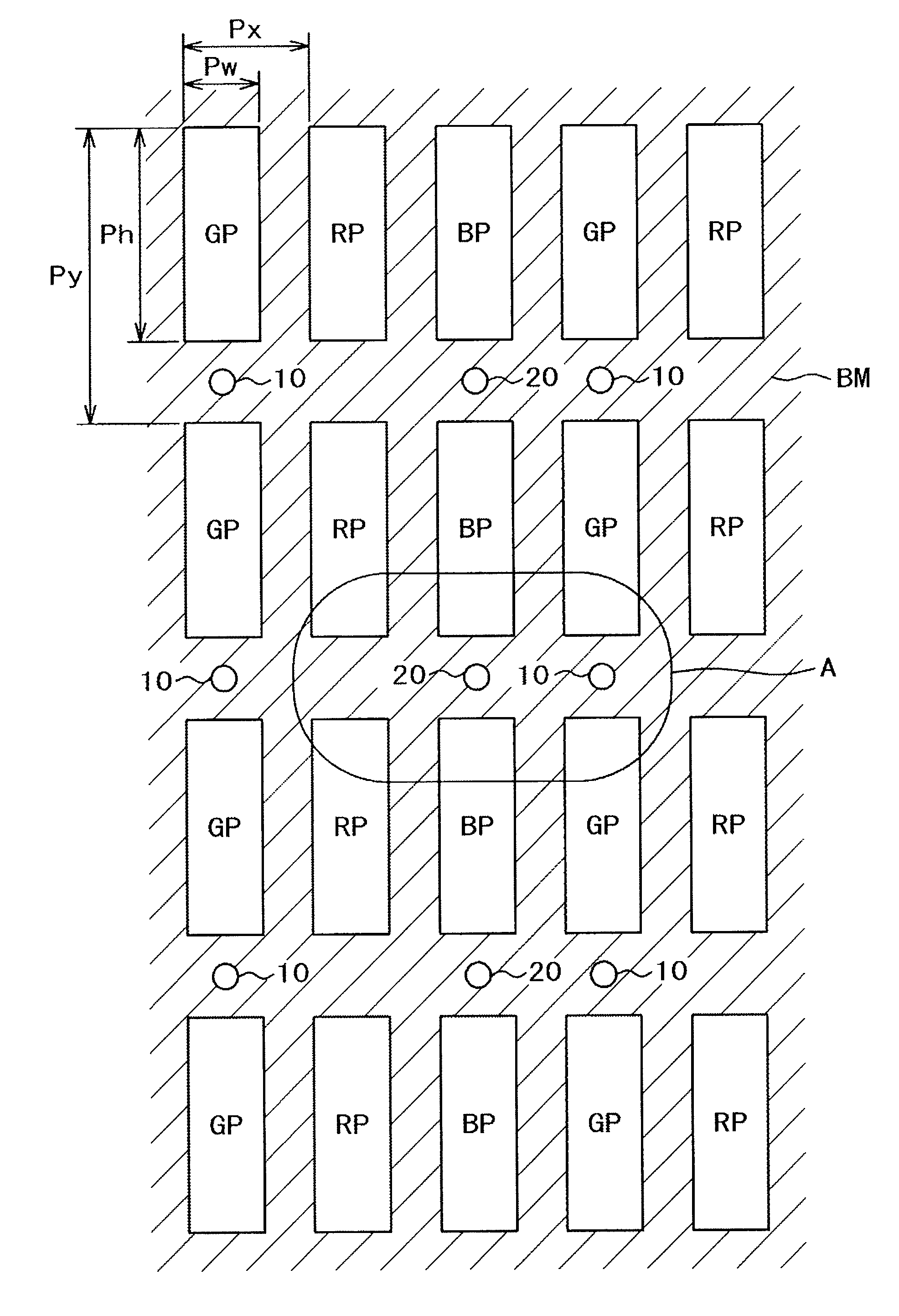
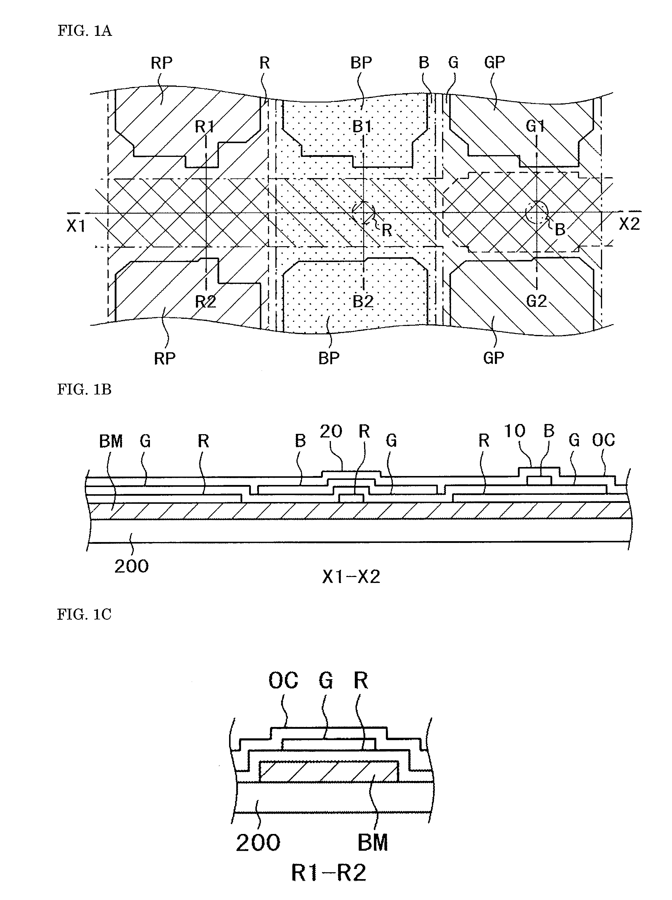
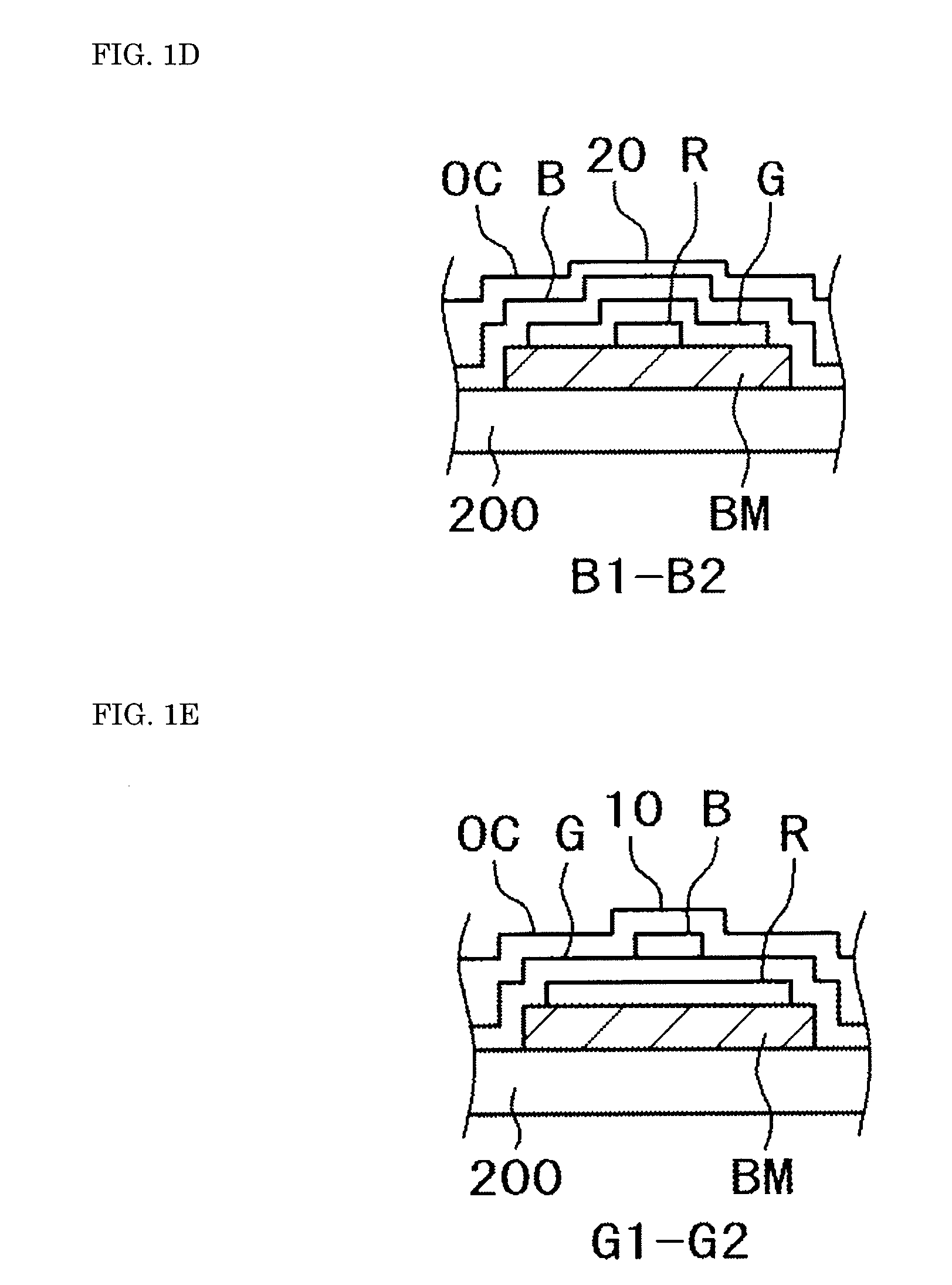
[0100]FIG. 1 is a diagram showing the first embodiment of the present invention. FIG. 1A is a diagram showing the details of the region A in FIG. 7. FIG. 1B is a cross sectional diagram along X1-X2 in FIG. 1A, FIG. 1C is a cross sectional diagram along R1-R2 in FIG. 1A, FIG. 1D is a cross sectional diagram along B1-B2 in FIG. 1A, and FIG. 1E is a cross sectional diagram along G1-G2 in FIG. 1A. The form of the pixel electrodes shown in FIGS. 1A to 1E reflects the actual pixel electrodes. In FIGS. 1A to 1E, pixels of the same color are aligned in the longitudinal direction, and pixels of different colors are aligned in the lateral direction.

[0101]As shown in FIGS. 1B, 1D and 1E, first spacers 10 are formed between the green pixels GP and second spacers 20 are formed between the blue pixels BP. These spacers are formed of color filters. As shown in FIG. 1B, the first spacers 10 are taller than the second spacers 20.

[0102]As shown in FIG. 1B, in a first spacer 10, a red color filter R i...

second embodiment

[0115]FIGS. 10A to 10E are diagrams showing the second embodiment of the present invention. FIG. 10A is a diagram showing the region A in FIG. 7 in detail. FIG. 10B is a cross sectional diagram along X1-X2 in FIG. 10A, FIG. 10C is a cross sectional diagram along R1-R2 in FIG. 10A, FIG. 10D is a cross sectional diagram along B1-B2 in FIG. 10A, and FIG. 10E is a cross sectional diagram along G1-G2 in FIG. 10A. The form of the pixel electrodes in FIGS. 10A to 10E reflects the actual pixel electrodes. In FIGS. 10A to 10E, pixels of the same color are aligned in the longitudinal direction, and pixels of different colors are aligned in the lateral direction.

[0116]As shown in FIGS. 10B, 10D and 10E, a first spacer 10 is formed between green pixels GP and a second spacer 20 is formed between blue pixels BP. These spacers are formed of color filters. As shown in FIG. 1B, the first spacer 10 is taller than the second spacer 20.

[0117]The present embodiment is different from the first embodimen...

third embodiment

[0123]As shown in FIG. 6, a peripheral light blocking film 220 in frame form is formed of a black matrix BM outside the display region 210 on the facing substrate 200 of the liquid crystal display panel. The outside of the wiring region 140 on the TFT substrate 100 side, where TFT's and wires for these are formed, corresponds to the peripheral light blocking film 220, and the space between the TFT substrate 100 and the facing substrate 200 is great relative to the display region 210. Accordingly, when spacers having the same height as in the display region 210 are formed in the portion of the peripheral light blocking film 220, the distance between the TFT substrate 100 and the facing substrate 200 becomes small and, as shown in FIG. 15, the TFT substrate 100 deforms in the periphery portion, for example. FIG. 15 shows an example where a peripheral spacer 30 is formed of a red color filter R in a stripe or covering the whole substrate and a blue color filter B in columnar form. In F...


PUM

PropertyMeasurementUnit
diameteraaaaaaaaaa
diameteraaaaaaaaaa
width Pwaaaaaaaaaa

Abstract

An object of the present invention is to form spacers for defining the space between the TFT substrate and the facing substrate of color filters, and by doing so, finely control the height of the spacers. First spacers 10 are formed of green color filters G in pillar form on top of red color filters R and blue color filters B (green color filters G) having a large area between blue pixels BP; second spacers 20 are formed by layering blue color filters B (green color filters G) and green color filters G having a large area on top of red color filters R in pillar form between green pixels GP; and the second spacers 20 are shorter than the first spacers 10 due to the leveling effects of the layered blue color filters B (green color filters G) and green color filters G.

Description

[0001]The present application claims priority over Japanese application JP2007-326080 filed on Dec. 18, 2007, the content of which is hereby incorporated into this application by reference.BACKGROUND OF THE INVENTION[0002](1) Field of the Invention[0003]The present invention relates to a technology for defining the space between a TFT substrate and a facing substrate in a liquid crystal display using a support pillar system.[0004](2) Related Art Statement[0005]In liquid crystal display devices, the space between the TFT substrate on which pixel electrodes and thin film transistors (TFT's) are formed and the facing substrate on which color filters and the like are formed is filled in with liquid crystal so that an image is formed by controlling the molecules of this liquid crystal by means of an electrical field. The space between the TFT substrate and the facing substrate is as small as several microns. It is extremely important to set an appropriate space between the TFT substrate ...

Claims


Application Information

Patent Timeline
Patent Type & Authority Applications(United States)
IPC IPC(8): G02F1/1339G02F1/1335
CPCG02F1/133514G02F2001/13396G02F1/13394G02F1/13396
Inventor IWATO, HIROAKIWATANABE, YOSHIKISHIRAI, NORIMICHIKANESAKA, KAZUMI
Owner PANASONIC LIQUID CRYSTAL DISPLAY CO LTD
Why Eureka
Try Eureka