Method for fabricating an integrated circuit comprising a three-dimensional capacitor

a three-dimensional capacitor and integrated circuit technology, applied in the field of integrated circuits, can solve problems such as the dispersion of the capacitive values of theoretically identical capacitors, and achieve the effect of reducing the access resistance of the capacitor

Active Publication Date: 2006-10-19
STMICROELECTRONICS SRL
View PDF23 Cites 21 Cited by
  • Summary
  • Abstract
  • Description
  • Claims
  • Application Information

AI Technical Summary

Benefits of technology

[0007] Embodiments of the present invention provide a solution to these problems, in particular by forming a metal layer which comes in contact with the bottom of the trenches and is both used as a stop layer for etching the trenches and partially short circuits the lower electrode of the capacitor. The etching height of the trenches is thus controlled from one batch to another, and the access resistance of the capacitor is reduced.

Problems solved by technology

It moreover proves difficult to ensure good etching reproducibility from one batch of wafers to another, which results in a dispersion of the capacitive values of theoretically identical capacitors.

Method used


Image

  • Method for fabricating an integrated circuit comprising a three-dimensional capacitor
  • Method for fabricating an integrated circuit comprising a three-dimensional capacitor
  • Method for fabricating an integrated circuit comprising a three-dimensional capacitor

Examples


Embodiment Construction

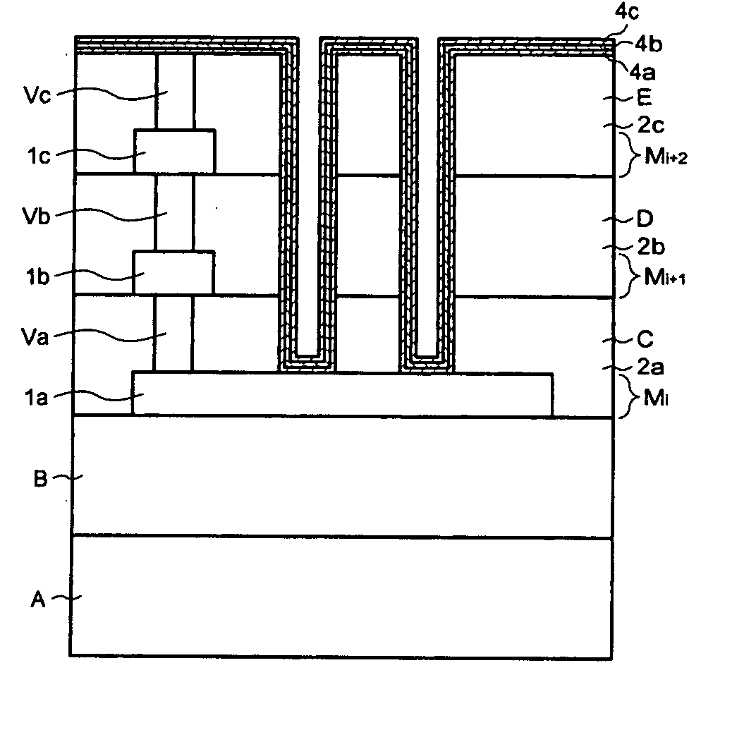
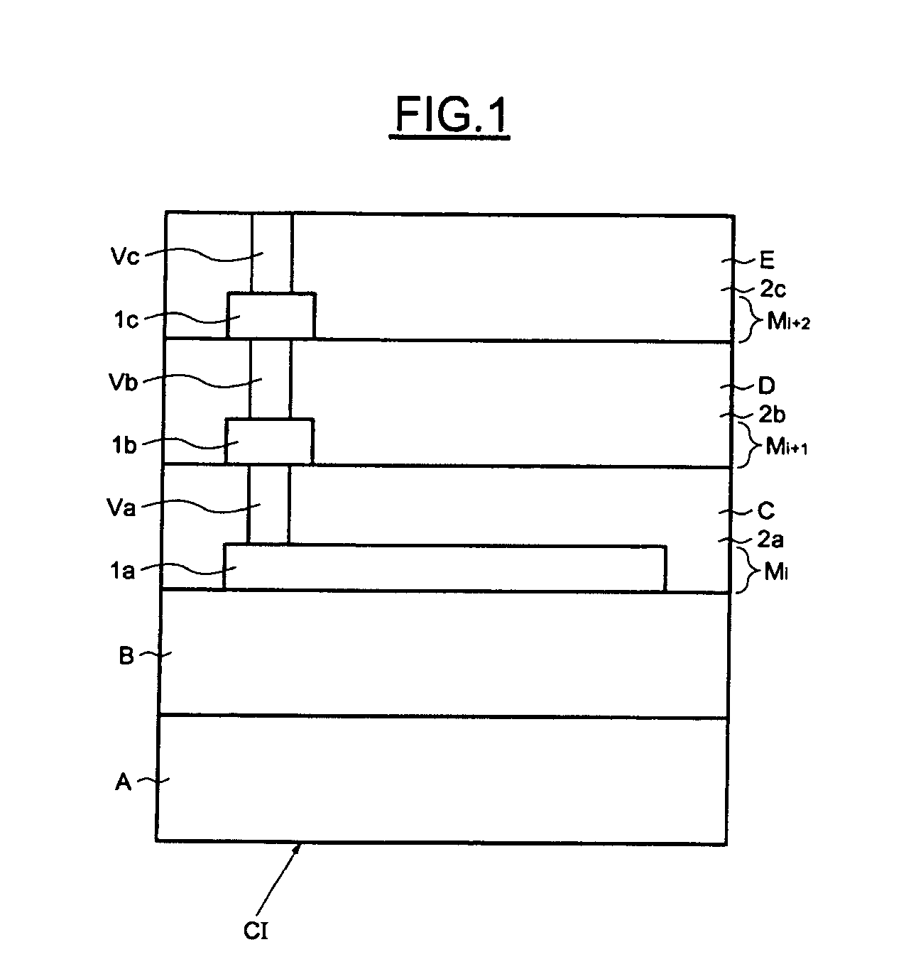
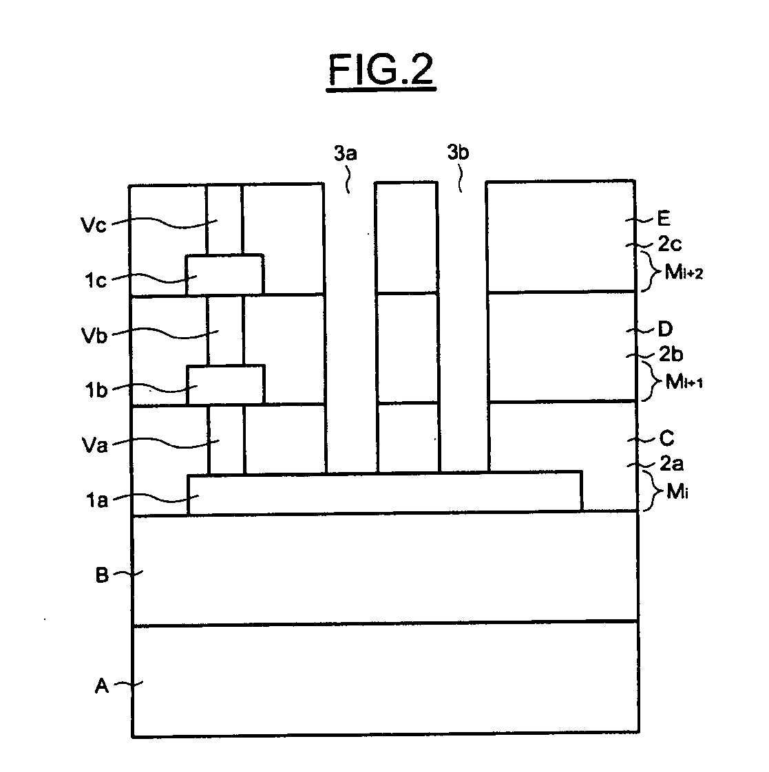
[0018]FIG. 1 represents an integrated circuit CI comprising a silicon substrate A on which a dielectric layer B has been deposited. A plurality of interconnection levels C, D and E rest on the dielectric layer B. Each interconnection level includes a metallization level formed by metal tracks and a level of vias, all of this coated in a dielectric material. The production of each interconnection level is conventional and known per se by those skilled in the art. In the example described here, the metallization level Mi of the interconnection level C comprises a metal layer 1a. The layer 1a may be of aluminum or copper. The metallization level Mi+1 of the interconnection level D comprises an interconnection line, or track 1b. The metallization level Mi+2 of the interconnection level E comprises an interconnection line, or track 1c. The interconnection lines 1a, 1b, 1c of the various interconnection levels C, D, E are connected to one another by the vias Va, Vb, Vc formed in the diele...


PUM

PropertyMeasurementUnit
distanceaaaaaaaaaa
conductiveaaaaaaaaaa
electricallyaaaaaaaaaa

Abstract

A capacitor fabricated, within an integrated circuit, has at least two capacitive trenches extending within a dielectric material. A metal layer is produced which is embedded in the dielectric material. To form the capacitor, the dielectric material is etched, with etching stopped at the metal layer so as to form the trenches. A layer of conductive material forming the lower electrode of the capacitor is then deposited at least on the sidewalls of the trenches and in contact with the metal layer. A dielectric layer is then deposited within the trenches. A layer of conductive material forming the upper electrode of the capacitor is then deposited within the trenches.

Description

PRIORITY CLAIM [0001] The present application claims priority from French Application for Patent No. 05 03894 filed Apr. 19, 2005, the disclosure of which is hereby incorporated by reference. BACKGROUND OF THE INVENTION [0002] 1. Technical Field of the Invention [0003] The present invention relates to integrated circuits and, more particularly, to integrated circuits comprising at least one three-dimensional capacitor. [0004] 2. Description of Related Art [0005] It is known to produce three-dimensional capacitors using an aluminum technology (reactive ion etching, RIE) or copper technology (Damascene). [0006] The three-dimensional capacitor is conventionally obtained by depositing a capacitive metal-insulator-metal (MIM) stack in which the lower layer is a conductive material, for example TiN. The insulator is a dielectric material of any permittivity (low, medium or high) and the upper electrode is a conductive material, for example TiN, in trenches which are obtained after etching...

Claims


Application Information

Patent Timeline
Patent Type & Authority Applications(United States)
IPC IPC(8): H01L21/20H01L21/8242
CPCH01L21/76838H01L21/76895H01L29/66181H01L28/40H01L28/91H01L23/5223H01L2924/0002H01L2924/00
Inventor GIRAUDIN, JEAN-CHRISTOPHECREMER, SEBASTIENDELPECH, PHILIPPE
Owner STMICROELECTRONICS SRL
Why Eureka
Try Eureka