

GaN enhanced MIS-HFET device and preparation method of same
An enhanced, device technology, applied in semiconductor/solid-state device manufacturing, semiconductor devices, electrical components, etc., can solve problems such as device reliability and stability, device threshold voltage that cannot meet the requirements of practical applications, and lattice damage , to achieve the effect of improving reliability and stability, increasing threshold voltage, and reducing access resistance
- Summary
- Abstract
- Description
- Claims
- Application Information
AI Technical Summary
Problems solved by technology
Method used
Image

Examples
Embodiment 1
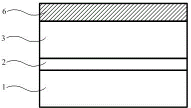
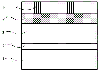
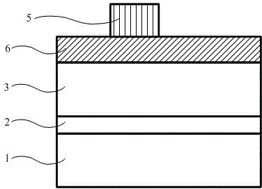
[0034] like Figure 9 Shown is a schematic structural diagram of the GaN enhanced MIS-HFET device of this embodiment, including a gate, a source, a drain, an insulating dielectric layer and a substrate 1 . The substrate usually chooses Si substrate or SiC substrate or sapphire substrate. A stress buffer layer 2 , a first GaN layer 3 and a selective growth layer are sequentially arranged on the substrate from bottom to top, and the selective growth layer includes a second GaN layer 7 and a heterogeneous layer 8 thereon. Wherein the first GaN layer is a high resistance GaN layer. The middle part of the selective growth layer has a through groove channel, and the bottom surface of the groove channel is covered with a p-type GaN layer 6 , the thickness of the p-type GaN layer 6 is less than or equal to the thickness of the second GaN layer 7 . Both sides of the upper surface of the heterogeneous layer 8 are covered with ohmic contact metal to form source and drain respectively. ...
Embodiment 2
[0047] like Figure 10 As shown, it is a schematic diagram of another structure of the GaN enhanced MIS-HFET device of the present invention, which is basically the same as the device structure of Example 1, the only difference is that when the heterogeneous layer is selectively grown, by modulating the N-type doping, That is, an N-type doped heterogeneous layer 13 is formed to further reduce the ohmic contact resistance of the source and drain regions and increase the current density of the device.
PUM
 Abstract
Description
Claims
Application Information