Method for preparing normally-off HEMT device through novel heterostructure magnesium diffusion
A heterostructure, normally-off technology, applied in the fields of semiconductor devices, semiconductor/solid-state device manufacturing, electrical components, etc., can solve the problems affecting the working performance of the device, the needs can not be well satisfied, the saturated output current is low, etc. The effect of gate leakage phenomenon, current density improvement, and saturation output current improvement
- Summary
- Abstract
- Description
- Claims
- Application Information
AI Technical Summary
Problems solved by technology
Method used
Image
Examples
Embodiment 1
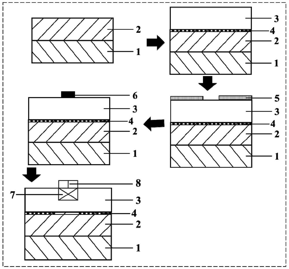
[0033] A method for preparing a normally-off HEMT device by diffusion of a new type of heterostructure magnesium in this embodiment is as follows (for the process flow, please refer to figure 1 shown):
[0034] (1) A layer of 7nm AlN material is grown on the GaN epitaxial wafer 2 base of the silicon substrate 1 as a barrier layer 3 by atomic layer deposition technology, and the new heterostructure forms a two-dimensional electron gas 4;
[0035] (2) Defining the structural shape of the magnesium grid strips on the GaN / AlN heterojunction material by photolithography using photoresist 5;
[0036] (3) Electron beam evaporation is used to deposit 50nm metal magnesium 6, and the magnesium grid strips are left by the stripping process;
[0037] (4) Thermal annealing is carried out in a vacuum rapid annealing furnace, the temperature of thermal annealing is 600°C, the annealing time is 5min, and the annealing atmosphere is a vacuum atmosphere lower than 0.1Pa to obtain a p-type dope...
Embodiment 2
[0042] A method of annealing and doping in this embodiment to realize a normally-off HEMT device is as follows:
[0043] (1) A layer of 1nm AlN material is grown on the GaN epitaxial wafer 2 substrate of the Si-based substrate 1 as a barrier layer 3 by atomic layer deposition technology, and the new heterostructure forms a two-dimensional electron gas 4;
[0044] (2) Defining the structural shape of the magnesium grid strips on the GaN / AlN heterojunction material by photolithography using photoresist 5;
[0045] (3) Electron beam evaporation is used to deposit 1nm metal magnesium 6, and the magnesium grid strips are left by the stripping process;
[0046] (4) Thermal annealing is carried out in a vacuum rapid annealing furnace. The thermal annealing temperature is 1000°C, the annealing time is 10min, and the annealing atmosphere is a vacuum atmosphere lower than 0.1Pa to obtain a p-type doped AlN material 7. Surface magnesium oxidation treatment is performed to obtain the MgO...
Embodiment 3
[0050] A method of annealing and doping in this embodiment to realize a normally-off HEMT device is as follows:
[0051] (1) A layer of 15nm AlN material is grown as a barrier layer 3 on the GaN epitaxial wafer 2 substrate of the Si-based substrate 1 by atomic layer deposition technology, and the new heterostructure forms a two-dimensional electron gas 4;
[0052] (2) Defining the structural shape of the magnesium grid strips on the GaN / AlN heterojunction material by photolithography using photoresist 5;
[0053] (3) Electron beam evaporation is used to deposit 100nm metal magnesium 6, and the magnesium grid strips are left by the stripping process;
[0054] (4) Thermal annealing is carried out in a vacuum rapid annealing furnace. The thermal annealing temperature is 200°C, the annealing time is 0.5min, and the annealing atmosphere is a vacuum atmosphere lower than 0.1Pa to obtain a p-type doped AlN material 7. The MgO passivation layer 8 is obtained by surface magnesium oxidat...
PUM
| Property | Measurement | Unit |
|---|---|---|
| thickness | aaaaa | aaaaa |
| thickness | aaaaa | aaaaa |
Abstract
Description
Claims
Application Information


