Nitride semiconductor device and method for manufacturing same

A technology of nitride semiconductors and manufacturing methods, which is applied in semiconductor/solid-state device manufacturing, semiconductor devices, electrical components, etc., can solve the problems that current density field effect transistors are difficult to achieve at the same time, achieve high current density, suppress thickness deviation, Effect of small gate leakage current

Inactive Publication Date: 2007-08-22
PANASONIC CORP
View PDF1 Cites 30 Cited by
  • Summary
  • Abstract
  • Description
  • Claims
  • Application Information

AI Technical Summary

Problems solved by technology

[0010] However, in order to make the conventional GaN-series electric field effect transistors very non-conductive, it is necessary to reduce the composition ratio of aluminum in the n-type AlGaN layer, or to thin the n-type AlGaN layer to reduce the pole. However, it is difficult to achieve both high current density and a very non-conductive electric field effect transistor at the same time.

Method used


Image

  • Nitride semiconductor device and method for manufacturing same
  • Nitride semiconductor device and method for manufacturing same
  • Nitride semiconductor device and method for manufacturing same

Examples


no. 1 example

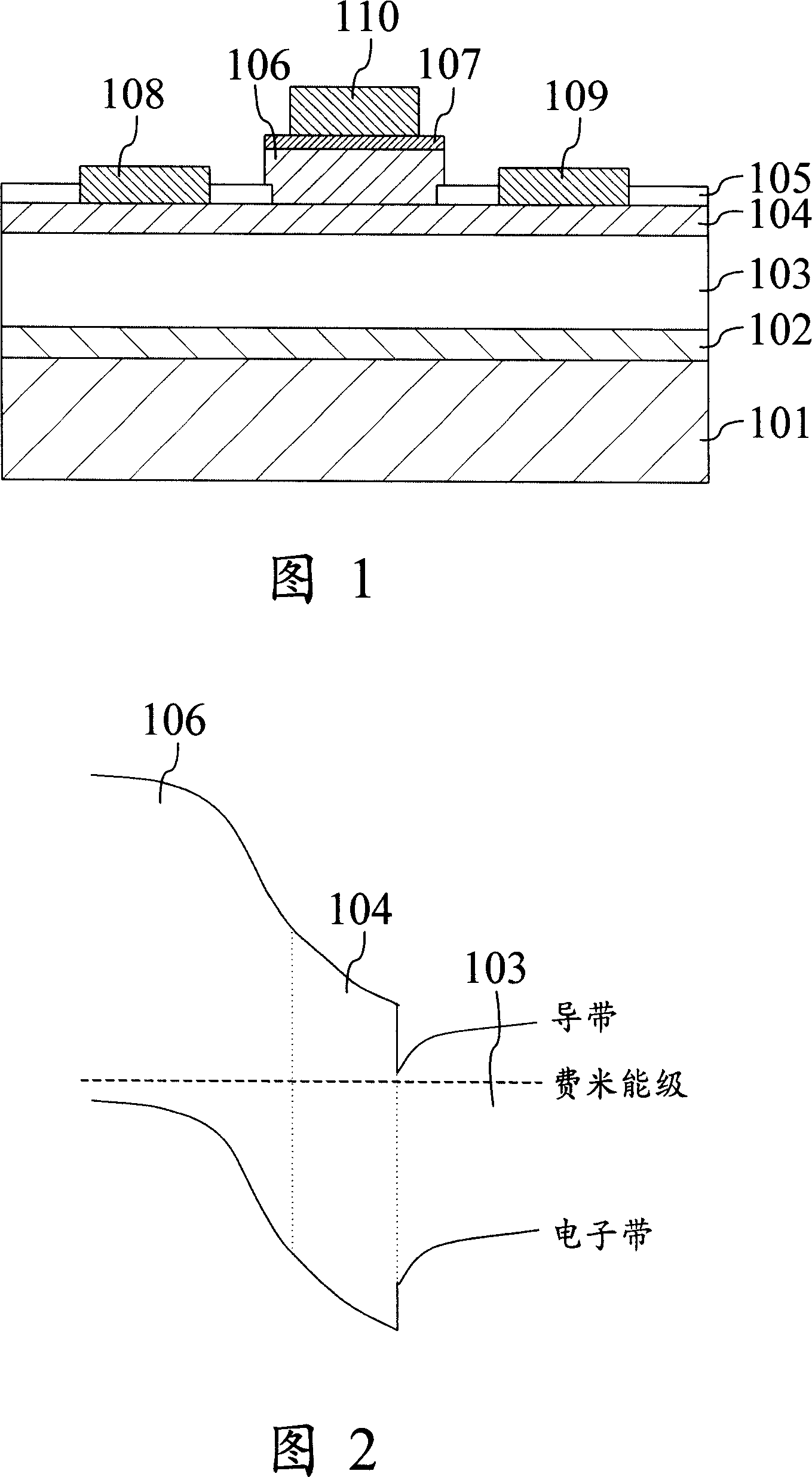
[0047] FIG. 1 is a cross-sectional view showing a nitride semiconductor device according to a first embodiment of the present invention. The nitride semiconductor device of this embodiment is a field effect transistor used as a high-power transistor.

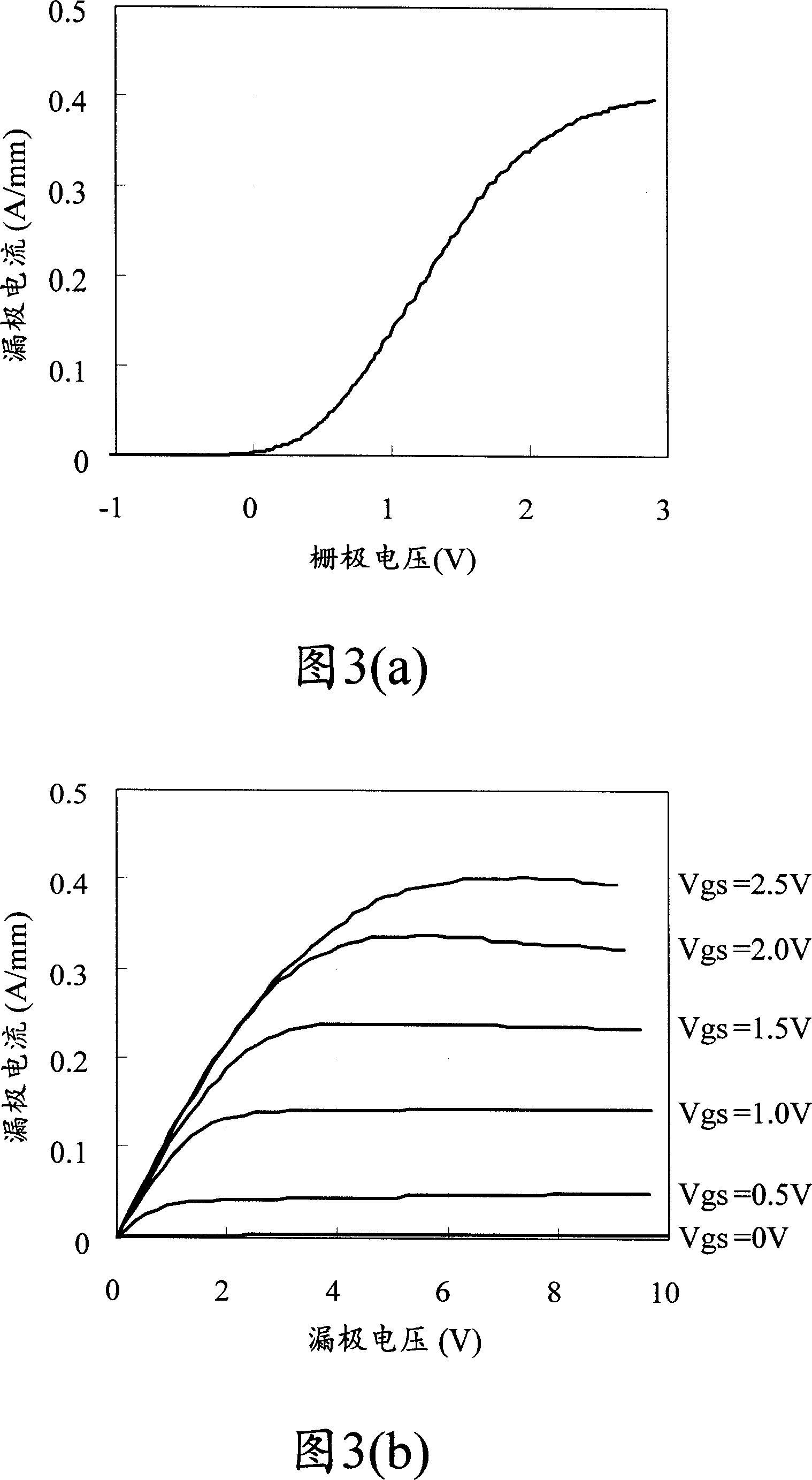
[0048] As shown in FIG. 1 , the nitride semiconductor device of the present embodiment includes: a sapphire substrate 101 with (0001) plane as the main surface; A nanometer aluminum nitride buffer layer 102; a non-doped gallium nitride layer 103 with a thickness of 2 microns on the aluminum nitride buffer layer 102; a thickness of 25 μm on the non-doped gallium nitride layer 103 A nanometer non-doped aluminum gallium nitride layer 104; a p-type aluminum gallium nitride layer 106 with a thickness of 100 nanometers set on a part of the non-doped aluminum gallium nitride layer 104; A high-concentration p-type gallium nitride layer 107 with a thickness of 5 nanometers is disposed on the layer 106 . Here, the so-called "non-doped" ...

no. 2 example

[0073] FIG. 6 is a cross-sectional view showing a nitride semiconductor device according to a second embodiment of the present invention.

[0074] As shown in this figure, the nitride semiconductor device of this embodiment includes: a sapphire substrate 601 with (0001) plane as the main surface; A nanometer aluminum nitride buffer layer 602, a non-doped gallium nitride layer 603 with a thickness of 2 micrometers, an undoped aluminum gallium nitride layer 604 with a thickness of 25 nanometers, a magnesium-doped aluminum alloy layer with a thickness of 5 nanometers The first p-type AlGaN layer 605 , the second p-type AlGaN layer 607 with a thickness of 100 nm and doped with Mg, and the high-concentration p-GaN layer 608 with a thickness of 5 nm. Here, in the nitride semiconductor device of this embodiment, the undoped aluminum gallium nitride layer 604, the first p-type aluminum gallium nitride layer 605, and the second p-type aluminum gallium nitride layer 607 are made of, for...


PUM

PropertyMeasurementUnit
thicknessaaaaaaaaaa
thicknessaaaaaaaaaa
thicknessaaaaaaaaaa

Abstract

A non-conductive type nitride semiconductor device capable of obtaining an enough current density is provided. An aluminium nitride buffer layer (602), a non-adulteration gallium nitride layer (603), a non-adulteration gallium aluminium nitride layer (604), a first p-type gallium aluminium nitride layer (605), a seond p-type gallium aluminium nitride layer (607), and a high concentration p-type gallium nitride layer (608) are orderly formed on a substrate (601), a gate electrode (611) is ohm contacted with the high concentration p-type gallium nitride layer. A source electrode (609) and a drain electrode (610) are provided on the non-adulteration gallium aluminium nitride layer. A pn knot generated by a two-dimensional electronic air generated on an interface between the non-adulteration gallium aluminium nitride layer and the non-adulteration gallium nitride layer and the first p-type gallium aluminium nitride layer and the second p-type gallium aluminium nitride layer. In addition, the second p-type gallium aluminium nitride layer covers a portion of a silicon nitride film (606).

Description

technical field [0001] The present invention relates to a nitride semiconductor device applicable to a high-power transistor used in a power supply circuit of a household appliance such as a television set. Background technique [0002] In recent years, research on a field effect transistor (FET=Field Effect Transistor) using a gallium nitride (GaN) series material as a high-frequency high-power device has been vigorously carried out. Because nitride semiconductor materials such as gallium nitride can be made into various mixed crystals with aluminum nitride (AlN) or indium nitride (InN), it is different from arsenic series such as gallium arsenide (GaAs) used in the past. Semiconductor materials can also form heterojunctions. However, in a heterojunction formed between nitride semiconductor layers, even in a state where no impurities are doped, a high concentration of carrier. Therefore, field effect transistors made of nitride semiconductors tend to be depleted (normall...

Claims


Application Information

Patent Timeline
Patent Type & Authority Applications(China)
IPC IPC(8): H01L29/772H01L21/335
CPCH01L29/432H01L29/7787H01L29/2003H01L29/66462H01L29/1066
Inventor 引田正洋柳原学上田哲三上本康裕田中毅
Owner PANASONIC CORP
Why Eureka
Try Eureka