Connecting materials and connecting structures

A technology for connecting materials and connecting parts, applied in the direction of connecting, welding/cutting media/materials, conductive materials, etc., can solve the problems of lowering melting point or sintering temperature and accumulation state, increasing surface area, etc., to suppress the generation of cracks, improve The effect of connection strength

Active Publication Date: 2021-09-24
SEKISUI CHEM CO LTD
View PDF9 Cites 0 Cited by
  • Summary
  • Abstract
  • Description
  • Claims
  • Application Information

AI Technical Summary

Problems solved by technology

[0003] In addition, it is known that when the particle size of metal particles is reduced to a size of 100 nm or less and the number of constituent atoms is reduced, the surface area ratio to the volume of the particles increases sharply, and the melting point or sintering temperature is significantly lower than that of the stacked state.

Method used


Image

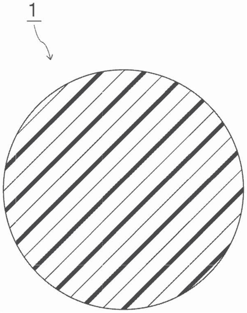
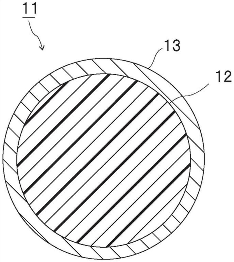
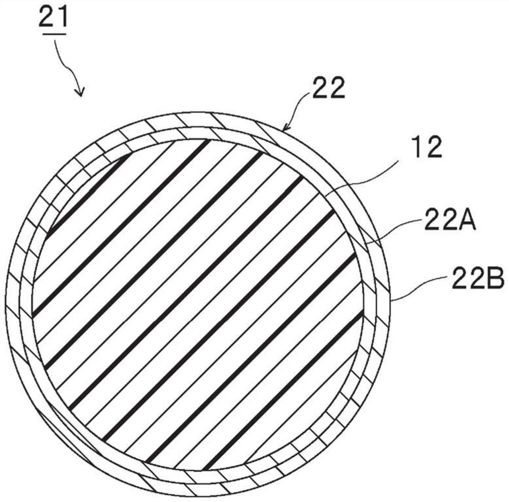
  • Connecting materials and connecting structures
  • Connecting materials and connecting structures
  • Connecting materials and connecting structures

Examples


Embodiment 1

[0171] (1) Production of polysiloxane oligomers

[0172] 1 part by weight of 1,3-divinyltetramethyldisiloxane (amount to be the weight % in the table) and 0.5% by weight of p-toluenesulfonic acid were placed in a 100 ml separable flask set in a warm bath 20 parts by weight of aqueous solution. After stirring at 40° C. for 1 hour, 0.05 parts by weight of sodium bicarbonate was added. Thereafter, 40 parts by weight of methylvinyldimethoxysilane (in the amount of weight % in the table), 10 parts by weight of methylphenyldimethoxysilane (in the amount of weight % in the table), methyl 10 weight part of trimethoxysilane (the quantity used as the weight% of a table|surface) was stirred for 1 hour. Thereafter, 1.9 parts by weight of a 10% by weight potassium hydroxide aqueous solution was added, and the mixture was stirred for 10 hours while the temperature was raised to 85° C. and the pressure was reduced by an aspirator, thereby performing a reaction. After the reaction, return ...

Embodiment 2~7、13~18 and comparative example 2~3

[0182] As shown in Tables 1 and 2, the polysiloxane monomer used for the production of polysiloxane oligomers was changed, the SPG pore diameter was changed as shown in Tables 1 and 2 below, and as shown in Tables 1 and 2 Except for changing the configurations of the particles and the linking material in this way, the particles X, the linking material, and the linking structure were produced in the same manner as in Example 1.

[0183] In addition, in Examples 17 and 18, the particle which has the electroconductive part shown in Table 2 was produced.

Embodiment 19

[0185] Dispersion C of Example 1 was prepared.

[0186]With respect to 100 parts by weight of the particles in the dispersion liquid C, 1 part by weight of methyltrimethoxysilane (manufactured by Shin-Etsu Chemical Co., Ltd. "KBM-13") was added, and ammonia in such an amount that the concentration of ammonia after the addition became 1% by weight The aqueous solution was stirred at room temperature for 24 hours, and then washed with water to obtain substrate particles. Particles X were obtained by subjecting the obtained substrate particles to a classification operation.

[0187] Except having used the obtained particle X, it carried out similarly to Example 1, and produced the connection material and connection structure.


PUM

PropertyMeasurementUnit
particle sizeaaaaaaaaaa

Abstract

The present invention provides a connecting material capable of suppressing the occurrence of cracks when a stress is applied to a connecting portion connecting two connecting parts, further suppressing variation in the thickness of the connecting portion, ensuring heat dissipation performance, and improving connection strength. . The connecting material of the present invention is a connecting material for connecting the connecting parts of two parts to be connected, and the connecting material includes particles and particles containing metal atoms, and the particles are used to form the connecting parts and make the connected parts The thickness of the connection part is less than twice the average particle diameter of the particles before connection, or the particles have an average particle diameter of not less than 1 μm and not more than 300 μm, and the particles have an average particle diameter of more than 3000 N / mm 2 And 20000N / mm 2 10% or less of the K value, the particles have a particle size CV value of 10% or less.

Description

technical field [0001] The present invention relates to a connection material that forms a connection portion that connects two connection object members. Moreover, this invention relates to the connection structure using the said connection material. Background technique [0002] In a non-insulated type semiconductor device which is one of power semiconductor devices used for an inverter or the like, a member fixing a semiconductor element is one of electrodes of the semiconductor device. For example, in a semiconductor device in which a power transistor is mounted on a fixed part using a Sn-Pb tie solder material, the fixed part (base material) that connects two connected parts is the collector of the power transistor. [0003] In addition, it is known that when the particle size of metal particles is reduced to a size of 100 nm or less and the number of constituent atoms is reduced, the surface area ratio to the volume of the particles increases sharply, and the melting ...

Claims


Application Information

Patent Timeline
Patent Type & Authority Patents(China)
IPC IPC(8): C09J201/00B22F7/08B23K35/24C08F12/36C08F16/32C08F30/08C08F36/08C08J3/12C09J9/02C09J11/00C09J11/08H01B1/00H01B1/22H01B5/00H01R11/01B22F1/05B22F1/052B22F1/10B22F1/18
CPCB22F7/08C08F16/32C08F30/08C08F36/08C08J3/12C09J9/02C09J11/00C09J201/00H01B1/22H01B5/00H01R11/01B22F7/064B23K35/0244C08K3/08C08K7/00C08K2003/0806C08K2003/0831C08K2003/085C08K2003/0862B23K35/262B23K35/3006B23K35/3013B23K35/302B23K35/3033B23K35/34B22F1/05B22F1/052B22F1/10B22F1/18C08L25/10B23K35/24
Inventor 山上舞羽根田聪胁屋武司山田恭幸上田沙织笹平昌男
Owner SEKISUI CHEM CO LTD
Why Eureka
Try Eureka