High-voltage integrated circuit device including high-voltage resistant diode

a high-voltage resistance, integrated circuit technology, applied in the direction of electronic switching, pulse technique, transportation and packaging, etc., can solve the problems of the high-voltage circuit region of the semiconductor device formed in the high-voltage circuit region 121/b> operating unstably

Active Publication Date: 2009-07-02
SEMICON COMPONENTS IND LLC
View PDF5 Cites 12 Cited by
  • Summary
  • Abstract
  • Description
  • Claims
  • Application Information

AI Technical Summary

Benefits of technology

[0017]The invention may be used in numerous circuits where power mosfets are controlled by low voltage logic circuits which turn on and off the gates of the power mosfets. Such circuits are often found in motor driver circuits, Class D amplifiers, and DC-DC converters. For example, in a ombined gate driver and bridge circuit, the bridge circuit has high side and low side power mosfets and low voltage gate drivers that turn the power mosfets on and off. The bootstrap diode protects the low power logic devices by blocking current from a bootstrap capacitor that is used to operate the power mosfets. The bootstrap diode appears works with the capacitor to not only prevent damaging high voltage / current from reaching the low voltage gate drivers but also allows the capacitor to store the charge for later use by the power mosfets.

Problems solved by technology

As a result, semiconductor devices formed in the high-voltage circuit regions 121 operate unstably due to the leakage currents.

Method used


Image

  • High-voltage integrated circuit device including high-voltage resistant diode
  • High-voltage integrated circuit device including high-voltage resistant diode
  • High-voltage integrated circuit device including high-voltage resistant diode

Examples


Embodiment Construction

[0026]The present invention will now be described more fully with reference to the accompanying drawings, in which exemplary embodiments of the invention are shown. The invention may, however, be embodied in many different forms and should not be construed as being limited to the embodiments set forth therein; rather, these embodiments are provided so that this disclosure will be thorough and complete, and will fully convey the concept of the invention to those skilled in the art. Like reference numerals in the drawings denote like elements, and thus their description will omitted.

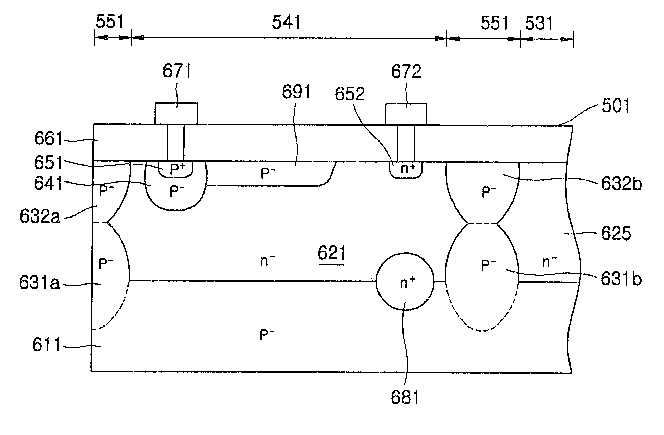
[0027]FIG. 5 is a schematic plan view of a high-voltage integrated circuit device 501 according to an embodiment of the present invention. Referring to FIG. 5, the high-voltage integrated circuit device 501 includes a low-voltage circuit region 511, a high-voltage circuit region 521, a junction termination 531, a high-voltage resistant diode 541, a first isolation region 551, and a second isolation region ...


PUM

PropertyMeasurementUnit
voltageaaaaaaaaaa
operating voltagesaaaaaaaaaa

Abstract

Provided is a high-voltage integrated circuit device including a high-voltage resistant diode. The device includes a low-voltage circuit region having a plurality of semiconductor devices, which operate with respect to a ground voltage, a high-voltage circuit region having a plurality of semiconductor devices, which operate with respect to a voltage that varies from the ground voltage to a high voltage, a junction termination and a first isolation region electrically isolating the low-voltage circuit region from the high-voltage circuit region, a high-voltage resistant diode formed between the low-voltage circuit region and the high-voltage circuit region, and a second isolation region surrounding the high-voltage resistant diode and electrically isolating the high-voltage resistant diode from the low-voltage circuit region and the high-voltage circuit region. Therefore, a leakage current of the high-voltage resistant diode can be prevented.

Description

CROSS-REFERENCE TO RELATED APPLICATIONS[0001]This application is a divisional of U.S. patent application Ser. No. 11 / 378,210 filed Mar. 16, 2006, which claims the priority of Korean Patent Application No. 2005-0021874, filed on Mar. 16, 2005, in the Korean Intellectual Property Office, the disclosure of which is incorporated herein in its entirety by reference.1. FIELD OF THE INVENTION[0002]The present invention relates to a high-voltage integrated circuit device, and more particularly, to a high-voltage integrated circuit device including a high-voltage resistant diode completely electrically isolated from other regions.2. DESCRIPTION OF THE RELATED ART[0003]Recently, technology for manufacturing a high-voltage integrated circuit devices including semiconductor devices operating at high voltages and lower voltage or logic circuits driving the semiconductor devices, has been developing rapidly. One example of such technology is shown in U.S. Pat. No. 6,507,085.[0004]FIGS. 1 through ...

Claims


Application Information

Patent Timeline
Patent Type & Authority Applications(United States)
IPC IPC(8): H01L27/06H01L29/93H01L23/58
CPCH01L27/0629H01L29/0634H01L29/0692H01L29/0878H01L29/1095H01L29/42368H01L29/7816H01L2924/0002H01L29/8611H01L29/868H03K17/6877H03K2217/0036H01L2924/00B60Y2200/147B62D53/06
Inventor KIM, SUNG-IYONGJEON, CHANG-KI
Owner SEMICON COMPONENTS IND LLC
Why Eureka
Try Eureka