Display substrate, display device including the display substrate and method of fabricating the display substrate

a technology of display substrate and substrate, which is applied in the direction of semiconductor devices, instruments, optics, etc., can solve the problems of low electron mobility of tfts formed of a-si:h, and achieve the effect of stable and reliable thin-film transistors

Inactive Publication Date: 2009-07-02
SAMSUNG ELECTRONICS CO LTD
View PDF5 Cites 71 Cited by
  • Summary
  • Abstract
  • Description
  • Claims
  • Application Information

AI Technical Summary

Benefits of technology

[0007]One aspect of the present invention provides a display substrate having stable and reliable thin-film transistors (“TFTs”).
[0008]Another aspect of the present invention also provides a display device including a display substrate having stable and reliable TFTs.
[0009]Yet another aspect of the present invention also provides a method of fabricating a display substrate having stable and reliable TFTs.

Problems solved by technology

However, TFTs formed of a-Si:H generally have low electron mobility.

Method used


Image

  • Display substrate, display device including the display substrate and method of fabricating the display substrate
  • Display substrate, display device including the display substrate and method of fabricating the display substrate
  • Display substrate, display device including the display substrate and method of fabricating the display substrate

Examples


Embodiment Construction

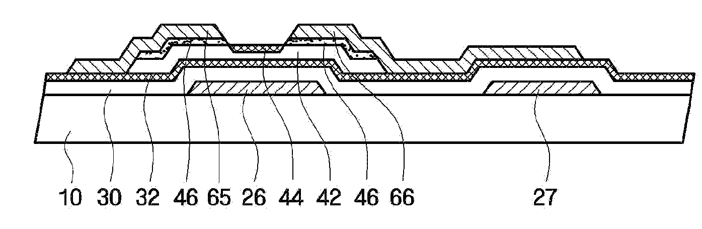
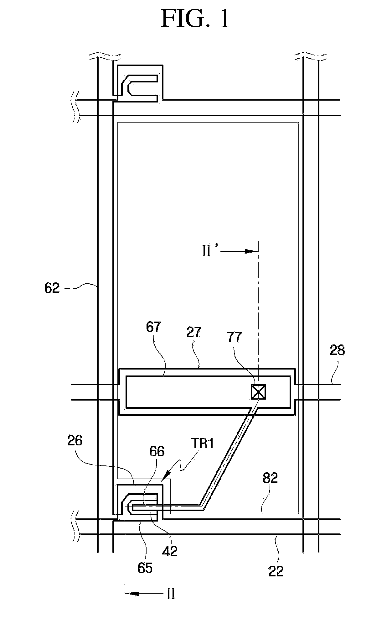
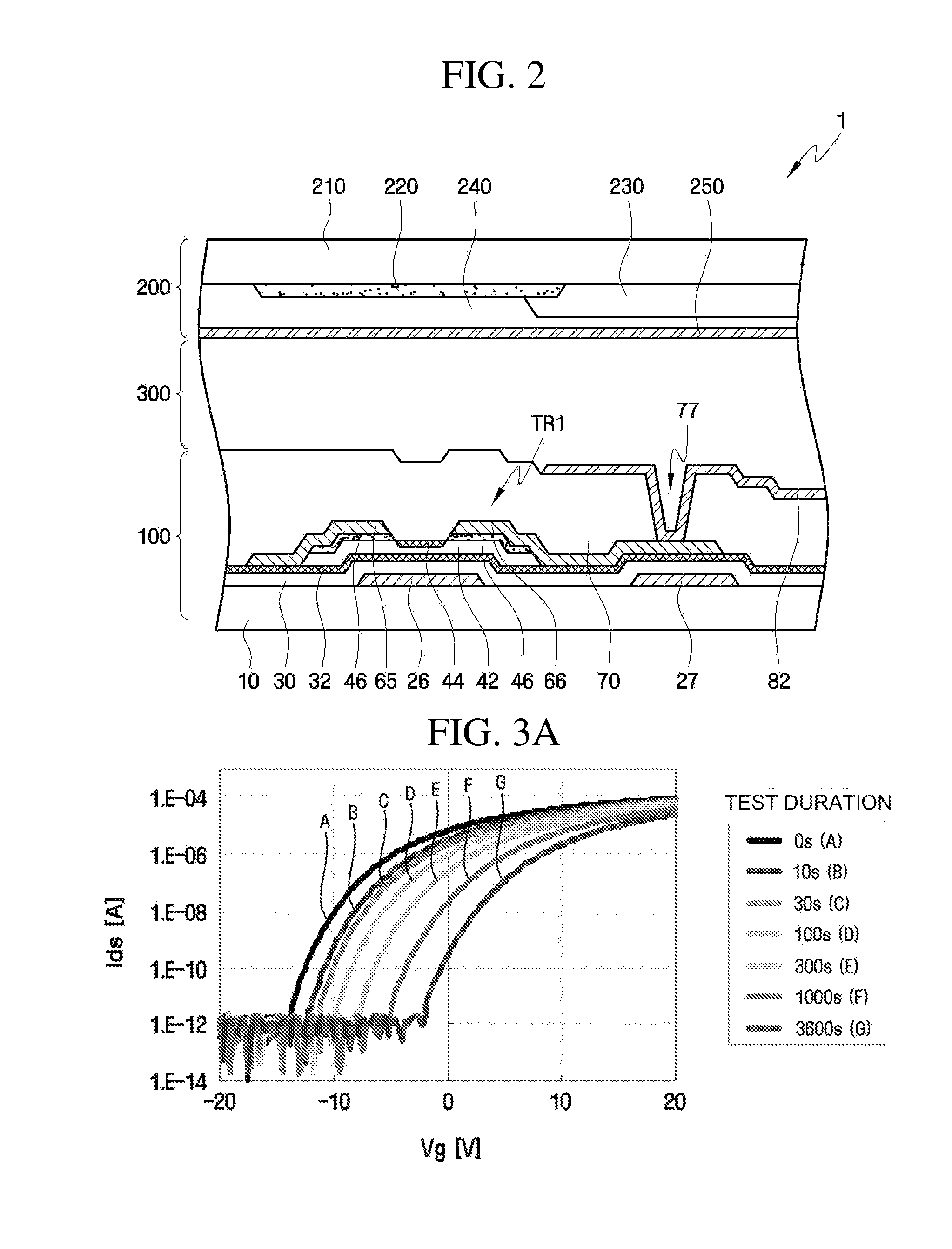
[0023]The present invention will now be described more fully with reference to the accompanying drawings, in which exemplary embodiments of the present invention are illustrated. Aspects, advantages and features of the present invention and methods of accomplishing the same may be understood more readily by reference to the following detailed description of exemplary embodiments and the accompanying drawings. The present invention may, however, be embodied in many different forms and should not be construed as being limited to the exemplary embodiments set forth herein. Rather, these exemplary embodiments are provided so that this disclosure will be thorough and complete and will fully convey the concept of the present invention to those skilled in the art, as defined by the appended claims. Like reference numerals refer to like elements throughout the specification.

[0024]It will be understood that when an element or layer is referred to as being “on”, “connected to” or “coupled to”...


PUM

PropertyMeasurementUnit
pressureaaaaaaaaaa
source-drain currentaaaaaaaaaa

Abstract

A display substrate, a display device including the display substrate, and a method of fabricating the display substrate are provided. The display substrate includes a gate electrode; a gate-insulating layer disposed on the gate electrode; an oxide semiconductor pattern disposed on the gate-insulating layer; a source electrode disposed on the oxide semiconductor pattern; and a drain electrode disposed on the oxide semiconductor pattern and separated from the source electrode, wherein at least one portion of at least one of the gate-insulating layer or the oxide semiconductor pattern is plasma-processed.

Description

[0001]This application claims priority to Korean Patent Application No. 10-2007-0137605, filed on Dec. 26, 2007, and all the benefits accruing therefrom under 35 U.S.C. §119, the contents of which in its entirety are herein incorporated by reference.BACKGROUND OF THE INVENTION[0002]1. Field of the Invention[0003]The present invention relates to a display substrate, a display device including the display substrate and a method of fabricating the display substrate. More particularly, the present invention relates to a display substrate, a display device including the display substrate and a method of fabricating the display substrate having stable and reliable thin-film transistors (“TFTs”)[0004]2. Description of the Related Art[0005]In recent years, the demand for the development of large-scale, high-quality display devices has steadily grown. In particular, the demand has been stronger than ever for improving the operating characteristics of thin-film transistors (“TFTs”) for drivin...

Claims


Application Information

Patent Timeline
Patent Type & Authority Applications(United States)
IPC IPC(8): G02F1/136H01L29/22H01L21/34
CPCH01L21/02554H01L29/7869H01L27/1225H01L21/02565G02F1/136
Inventor CHOI, JAE-HOYANG, SUNG-HOONYOON, KAP-SOOKIM, SUNG-RYULOH, HWA-YEULCHOI, YONG-MO
Owner SAMSUNG ELECTRONICS CO LTD
Why Eureka
Try Eureka