
PCB supporting woven fabric and a PCB having the same

a technology of woven fabric and pcb, which is applied in the direction of weaving, printed circuit non-printed electric components association, high frequency circuit adaptation, etc., can solve the problems of reducing the efficiency of pcb, slowing the speed of transmitting signals through conductive trace, and unavoidable placement of conductive traces on bumps, so as to improve the effectiveness and speed of signal transmission and reduce the number of bumps

Inactive Publication Date: 2009-07-30
INVENTEC CORP
View PDF2 Cites 5 Cited by
  • Summary
  • Abstract
  • Description
  • Claims
  • Application Information

AI Technical Summary

Benefits of technology

[0006]It is therefore an objective of the present invention to present a PCB supporting woven fabric and a PCB having the same to improve signals in effectiveness and speed of transmission.
[0009]Therefore, The supporting woven fabric in this invention aims to decrease the number of the bumps bulged thereof, thus to make the PCB improved in effectiveness and speed of signal transmission.

Problems solved by technology

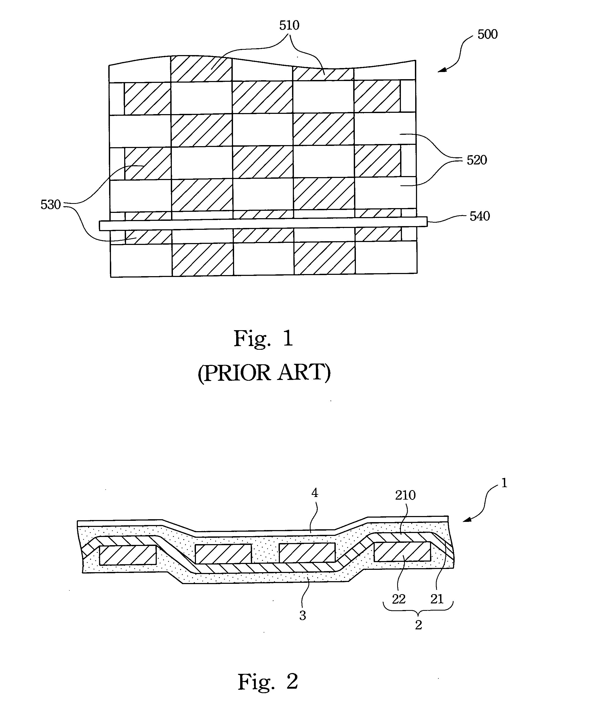
However, after the fiberglass weaving work 500 is processed to be a PCB, thousands of conductive traces are plated on the PCB and because every warp 510 that crosses over the weft 520 will respectively forms a bump upwardly on the fiberglass weaving work 500, some of those conductive traces will unavoidably be arranged to lie on the bumps.
The bumps may weaken the power and slow the speed of transmitting signals through the conductive trace thereon to provide bad performance.

Method used


Image

  • PCB supporting woven fabric and a PCB having the same
  • PCB supporting woven fabric and a PCB having the same
  • PCB supporting woven fabric and a PCB having the same

Examples


Embodiment Construction

[0016]Reference will now be made in detail to the present embodiments of the invention, examples of which are illustrated in the accompanying drawings. Wherever possible, the same reference numbers are used in the drawings and the description to refer to the same or like parts.

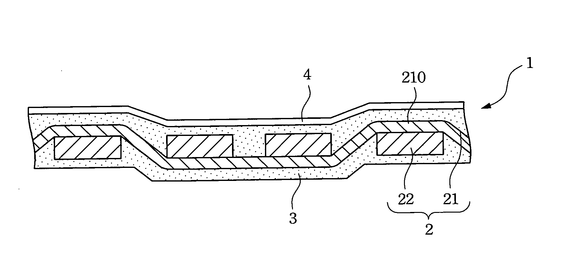
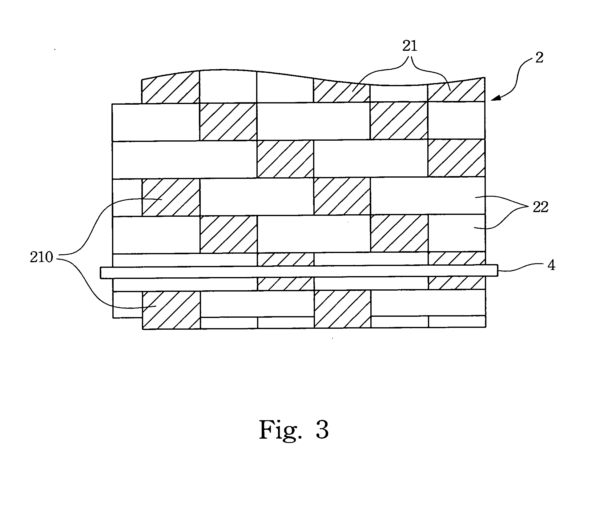
[0017]Referring to FIG. 1, a section view of a PCB according to the present invention, the printed circuit board (called PCB1 as follows) that we discussed in this invention, only implies to one of multiple layers of a finished PCB product. The PCB 1 mainly includes a supporting woven fabric 2, a filling resin body 3 and at least one signal trace 4. The supporting woven fabric 2 is made by vertically interlacing a number of first fiberglass strands from warp direction and a number of second fiberglass strands from weft direction with each other. In this invention the first fiberglass strands from warp direction are named as warp fiberglass strands 21, and the second fiberglass strands from weft direction are n...


PUM

PropertyMeasurementUnit
Speedaaaaaaaaaa

Abstract

The present invention is to provide a printed circuit board (PCB) supporting woven fabric and a PCB having the same. The PCB includes a supporting woven fabric, a filling resin body enveloping the supporting woven fabric and at least one signal trace arranged on the surface of the filling resin body. The supporting woven fabric is made by a number of warp fiberglass strands and weft fiberglass strands interlaced mutually, wherein each of the warp fiberglass strands initially crosses above one weft fiberglass strand to separately form a bump upwardly and passes through under the next at least two weft fiberglass strands. The invention aims to decrease the number of the bumps bulged thereof to make the PCB improved in effectiveness and speed of signal transmission.

Description

BACKGROUND[0001]1. Field of Invention[0002]This invention is related to a printed circuit board (PCB) and more particularly to a PCB with a supporting woven fabric to reduce the quantity of bumps formed on the supporting woven fabric.[0003]2. Description of Related Art[0004]A supporting board in a printed circuit board (PCB) used for upholding objects thereon is traditionally made by a piece of paper enveloped in resin. Nowadays, Referring to FIG. 1 a plain schematic diagram of a conventional fiberglass woven fabric, the supporting board of the PCB can be a fiberglass weaving work 500. The fiberglass weaving work 500 is woven by a plurality of fiberglass strands with longitudinal direction (called warp 510 as follows) interlaced through a plurality of fiberglass strands with latitudinal direction (called weft 520 as follows) wherein the warps 510 in an order of odd numbers are interlaced through every weft 520 by a rule of passing under one weft 520 first and then crossing over next...

Claims


Application Information

Patent Timeline
IPC IPC(8): H05K1/03D03D1/00B32B5/12B32B27/04
CPCD03D1/0082D03D15/0011H05K1/024H05K1/0366Y10T428/24917Y10S428/901Y10T428/24074Y10T428/2915Y10T428/24612H05K2201/029D03D15/267Y10T442/2992Y10T442/30Y10T442/3301Y10T442/3309
Inventor CHUANG, MU-CHIH
Owner INVENTEC CORP
Learn More