Array substrate and display device
- Summary
- Abstract
- Description
- Claims
- Application Information
AI Technical Summary
Benefits of technology
Problems solved by technology
Method used
Image

Examples
embodiment 1
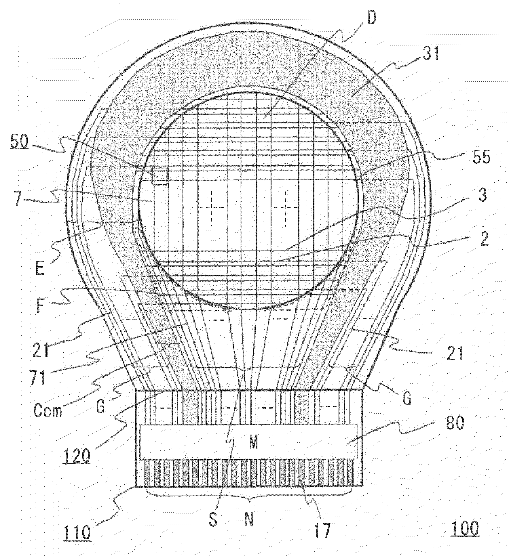
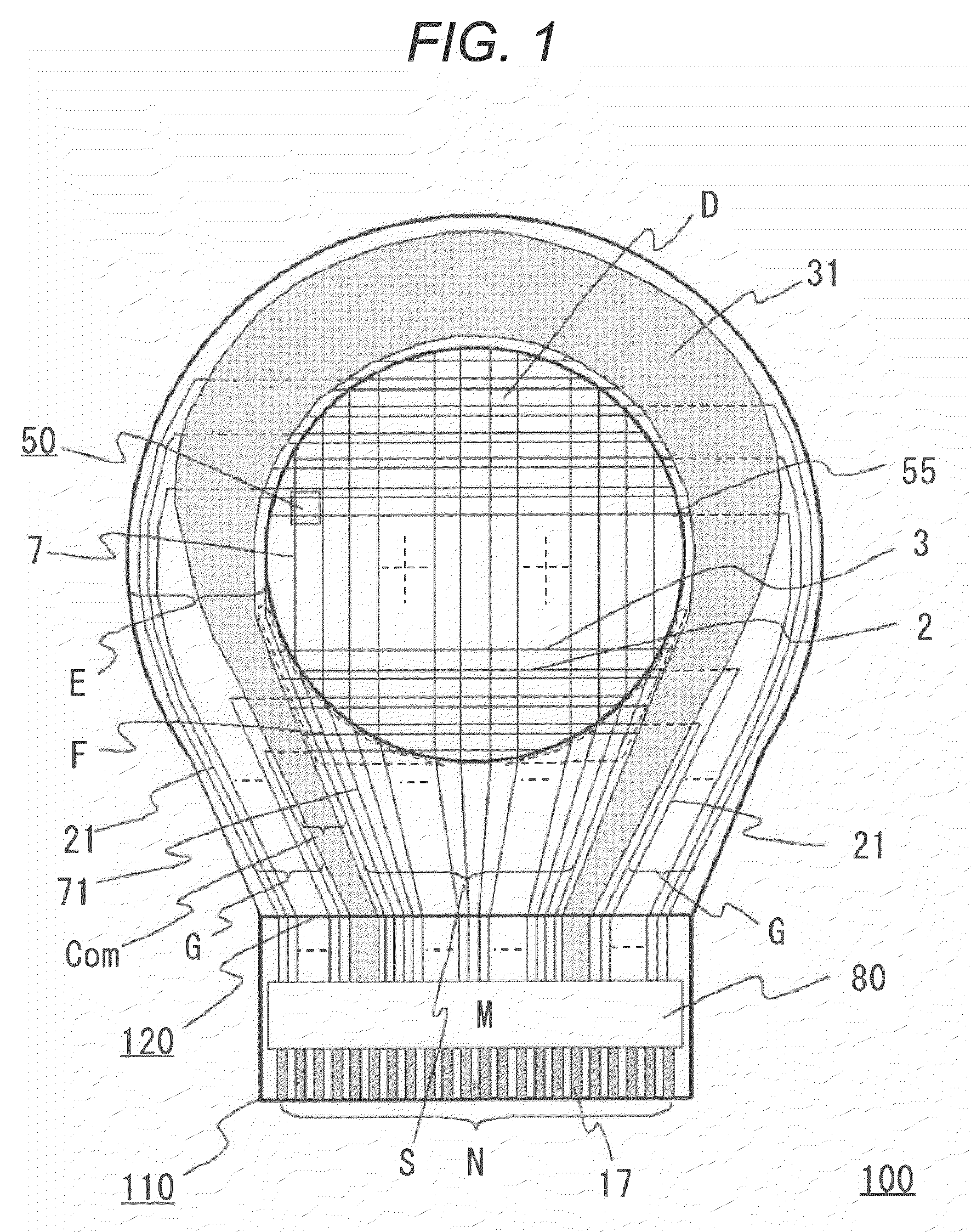
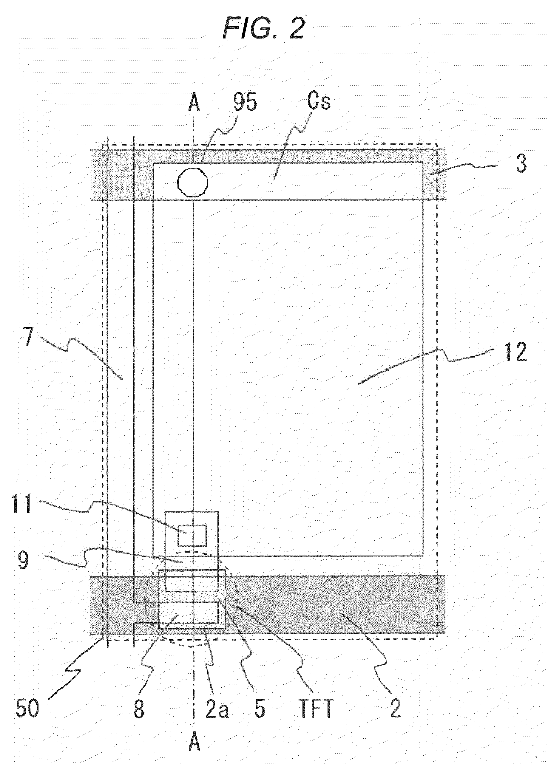
[0026]FIG. 1 is a plan view schematically illustrating a configuration of a display device according to Embodiment 1 of the present invention. FIG. 2 is an enlarged plan view illustrating one pixel which forms a display region of the display device shown in FIG. 1. FIG. 3 is a cross-sectional view taken along line A-A of FIG. 2.
[0027]Referring to FIG. 1, a liquid crystal display device 100 is configured such that a pixel 50 is formed in a region surrounded by a scanning line 2 and a signal line 7 which intersects the scanning line 2. An array substrate 110 having a non-quadrangle display region D where plural pixels 50 are disposed in a matrix-like shape is bonded to an opposing substrate 120 disposed opposite to the array substrate 110 by the use of a seal material with a spacing therebetween by a spacer. A liquid crystal is enclosed in the spacing. Further, as it is described below, in a transmission type liquid crystal display device 100, a backlight is disposed on the rear surfa...
embodiment 2
[0063]FIG. 6 is an enlarged plan view illustrating the frame region in the array substrate of the liquid crystal display device according to Embodiment 2 of the present invention. FIG. 7 is a cross-sectional view taken along line C-C of FIG. 6.
[0064]In Embodiment 1, the common lead-out line 31 bypassed the intersection region F and was disposed in the region Com between the region G of the scanning lead-out line 21 and the region S of the signal lead-out line 71. However, in Embodiment 2, as shown in FIG. 6, the common lead-out line 31 bypasses the intersection region F and the region Com is disposed at a position nearer to the end of the array substrate 110 than the region G of the scanning lead-out line 21 and the region S of the signal lead-out line 71. Therefore, the common lead-out line 31 is disposed not to intersect either the scanning lead-out line 21 or the signal lead-out line 71.
[0065]In Embodiment 2, in order to connect the sub-capacitance line 3 formed on the first cond...
embodiment 3
[0073]FIG. 8 is a plan view schematically illustrating a configuration of a display device according to Embodiment 3 of the present invention. Similar to Embodiment 2, the common lead-out line 31 extending from a driver IC which is a driving circuit 80 is disposed in a region Com1 in the frame region E close to the end of the array substrate 110, where the region Com1 does not intersect the both the scanning lead-out line 21 and the signal lead-out line 71. Further, similar to Embodiment 1, the common lead-out line 31 is disposed in a region Com2 between the region G of the scanning lead-out line 21 and the region S of the signal lead-out line 71, where the region Com2 is formed in a region which is turned back and extended from the frame region E opposite to the driving circuit 80 with respect to the display region D toward the driving circuit 80.
[0074]The reason for such configuration is that since an output terminal applying the common potential (reference potential) is located a...
PUM
 Abstract
Description
Claims
Application Information
 - Generate Ideas
- Intellectual Property
- Life Sciences
- Materials
- Tech Scout
- Unparalleled Data Quality
- Higher Quality Content
- 60% Fewer Hallucinations
Browse by: Latest US Patents, China's latest patents, Technical Efficacy Thesaurus, Application Domain, Technology Topic, Popular Technical Reports.
© 2025 PatSnap. All rights reserved.Legal|Privacy policy|Modern Slavery Act Transparency Statement|Sitemap|About US| Contact US: help@patsnap.com