Light Emitting Device Mounting Substrate, Light Emitting Device Housing Package, Light Emitting Apparatus, and Illuminating Apparatus

a technology for light emitting devices and mounting substrates, which is applied in semiconductor devices, electrical devices, semiconductor/solid-state device details, etc., can solve problems such as deterioration in luminous efficiency, and achieve the effect of reducing heat transmission and reducing heat dissipation efficiency

Inactive Publication Date: 2009-08-13
KYOCERA CORP
View PDF10 Cites 39 Cited by
  • Summary
  • Abstract
  • Description
  • Claims
  • Application Information

AI Technical Summary

Benefits of technology

[0005]The invention has been devised in view of the above-described problem with the conventional art, and accordingly its object is to provide a light-emitting apparatus that succeeds in dissipating heat transmitted to a specific electrode of a light-emitting device with higher heat-dissipation efficiency.

Problems solved by technology

If the light-emitting device undergoes accumulation of heat and an ensuing significant temperature rise, there arises a problem of deterioration in luminous efficiency.

Method used


Image

  • Light Emitting Device Mounting Substrate, Light Emitting Device Housing Package, Light Emitting Apparatus, and Illuminating Apparatus
  • Light Emitting Device Mounting Substrate, Light Emitting Device Housing Package, Light Emitting Apparatus, and Illuminating Apparatus
  • Light Emitting Device Mounting Substrate, Light Emitting Device Housing Package, Light Emitting Apparatus, and Illuminating Apparatus

Examples


first embodiment

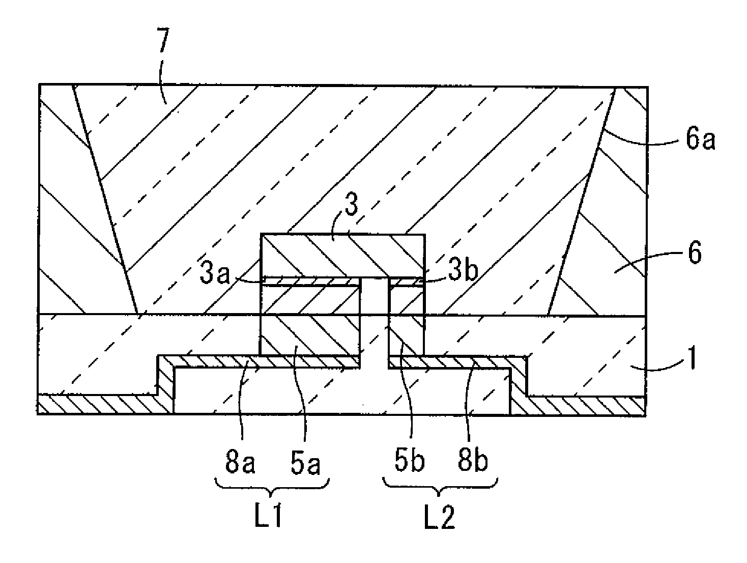
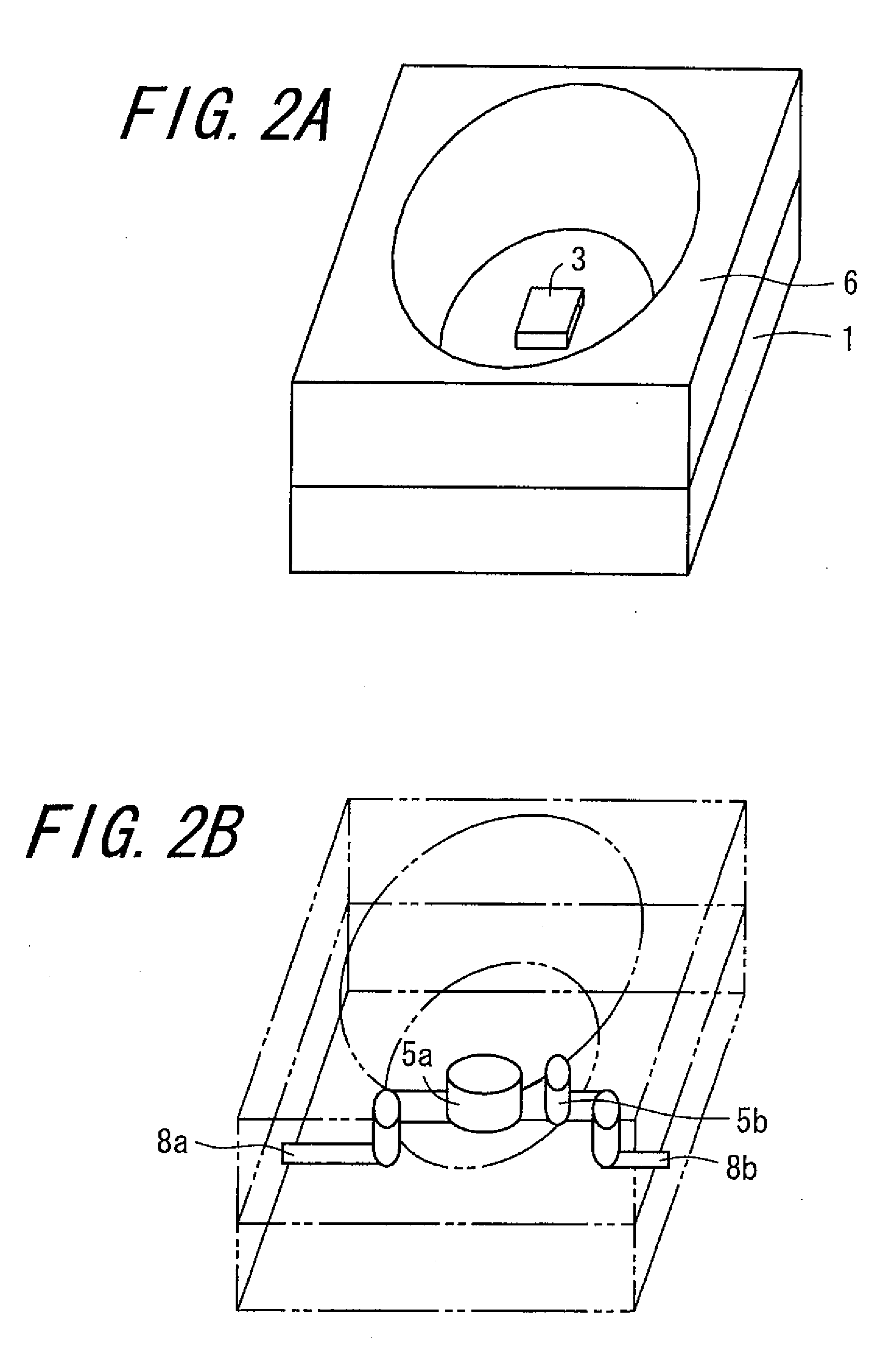
[0099]FIGS. 1A and 1B are sectional views showing a light-emitting apparatus incorporating a light-emitting device mounting substrate in accordance with a first embodiment of the invention. FIG. 2A is a perspective view of the light-emitting apparatus depicted in FIG. 1A. FIG. 2B is a perspective transparent view showing the configuration of a first and a second electrically conductive path of the light-emitting apparatus depicted in FIG. 1A.

[0100]As shown in FIG. 1A, in the light-emitting apparatus of the first embodiment, a light-emitting device 3 is mounted inside an opening formed in a light-emitting device housing package. Moreover, a light-transmittable member 7 is disposed inside the opening of the package so as to cover the light-emitting device 3. The light-emitting device housing package is composed of a light-emitting device mounting substrate and a light reflection portion 6 disposed on a surface of the light-emitting device mounting substrate so as to surround the regio...

second embodiment

[0136]FIGS. 5A and 5B are sectional views showing a light-emitting device mounting substrate and a light-emitting apparatus incorporating the substrate in accordance with a second embodiment of the invention. FIG. 6 is a sectional perspective view of the construction depicted in FIG. 5A.

[0137]As shown in FIG. 5A, in the light-emitting apparatus of the second embodiment, a light-emitting device 3 is mounted inside an opening formed in a light-emitting device housing package. Moreover, a light-transmittable member 7 is disposed inside the opening of the package so as to cover the light-emitting device 3. The light-emitting device housing package is composed of a light-emitting device mounting substrate and a light reflection portion 6 disposed on a surface of the light-emitting device mounting substrate so as to surround the region in which is mounted the light-emitting device 3.

[0138]The light-emitting device mounting substrate is composed of a base body 1 which mounts thereon the li...

third embodiment

[0153]FIGS. 7A and 7B are sectional views showing a light-emitting device mounting substrate and a light-emitting apparatus incorporating the substrate in accordance with a third embodiment of the invention. FIG. 8 is a sectional perspective view of the construction depicted in FIG. 7A.

[0154]As shown in FIG. 7A, in the light-emitting apparatus of the third embodiment, a light-emitting device 3 is mounted inside an opening formed in a light-emitting device housing package. Moreover, a light-transmittable member 7 is disposed inside the opening of the package so as to cover the light-emitting device 3. The light-emitting device housing package is composed of a light-emitting device mounting substrate and a light reflection portion 6 disposed on a surface of the light-emitting device mounting substrate so as to surround the region in which is mounted the light-emitting device 3.

[0155]The light-emitting device mounting substrate is composed of a base body 1 which mounts thereon the ligh...


PUM


Abstract

A light-emitting apparatus with improved dissipation efficiency of heat transmitted to a specific electrode of a light-emitting device is provided. A light-emitting device mounting substrate used for the light emitting apparatus include a base body (1) which mounts thereon a light-emitting device (3); a first electrically conductive path (L1) formed within the base body (1), one end thereof being electrically connected to a first electrode (3a) of the light-emitting device (3) and the other end thereof being led out to a surface of the base body (1); and a second electrically conductive path (L2) formed in the base body (1), one end thereof being electrically connected to a second electrode (3b) of the light-emitting device (3), and the other end thereof being formed on the surface of the base body (1). The first electrically conductive path (L1) is made smaller in thermal resistance than the second electrically conductive path (L2).

Description

TECHNICAL FIELD[0001]The present invention relates to a substrate for mounting thereon a light-emitting device such as a light-emitting diode (LED for short), a package for housing a light-emitting device, and a light-emitting apparatus, as well as to an illuminating apparatus incorporating such components.BACKGROUND ART[0002]In a light-emitting apparatus of conventional design, a light-emitting device such as a light-emitting diode is mounted on a base body, and is provided with a reflection surface so as to surround the light-emitting device. Moreover, an inside of the reflection surface is filled with a light-transmittable member so as to cover the light-emitting device. On the light-emitting device is formed a wavelength converting layer containing a phosphor for converting the wavelength of light emitted from the light-emitting device. The base body is provided with an electrically conductive path formed of a wiring conductor or a via conductor that is electrically connected to...

Claims


Application Information

Patent Timeline
Patent Type & Authority Applications(United States)
IPC IPC(8): H01L33/00H01L33/62H01L33/64
CPCH01L23/055H01L23/3107H01L33/62H01L33/642H01L33/647H01L2924/12041H01L2924/01025H01L2924/01078H01L2924/01079H01L2924/09701H01L2224/16
Inventor MORI, YUKISEKINE, FUMIAKI
Owner KYOCERA CORP
Why Eureka
Try Eureka