Planar Illumination Device and Manufacturing Method of Same

a planar illumination and manufacturing method technology, applied in the direction of lighting and heating apparatus, instruments, optical elements, etc., can solve the problems of reducing the light emitting efficiency of the led by temperature rise, increasing the heat amount generated by the led, etc., and achieves high brightness of the planar illumination device, improved workability of the heat conduction agent filling work, and efficient radiation

Inactive Publication Date: 2009-08-13
MINEBEA CO LTD
View PDF5 Cites 45 Cited by
  • Summary
  • Abstract
  • Description
  • Claims
  • Application Information

AI Technical Summary

Problems solved by technology

However, when the electric current supplied to the LED or the number thereof is increased, a heat amount generated from the LED is also increased and there is a problem that light emitting efficiency of the LED is lowered by temperature rise.

Method used


Image

  • Planar Illumination Device and Manufacturing Method of Same
  • Planar Illumination Device and Manufacturing Method of Same
  • Planar Illumination Device and Manufacturing Method of Same

Examples


first embodiment

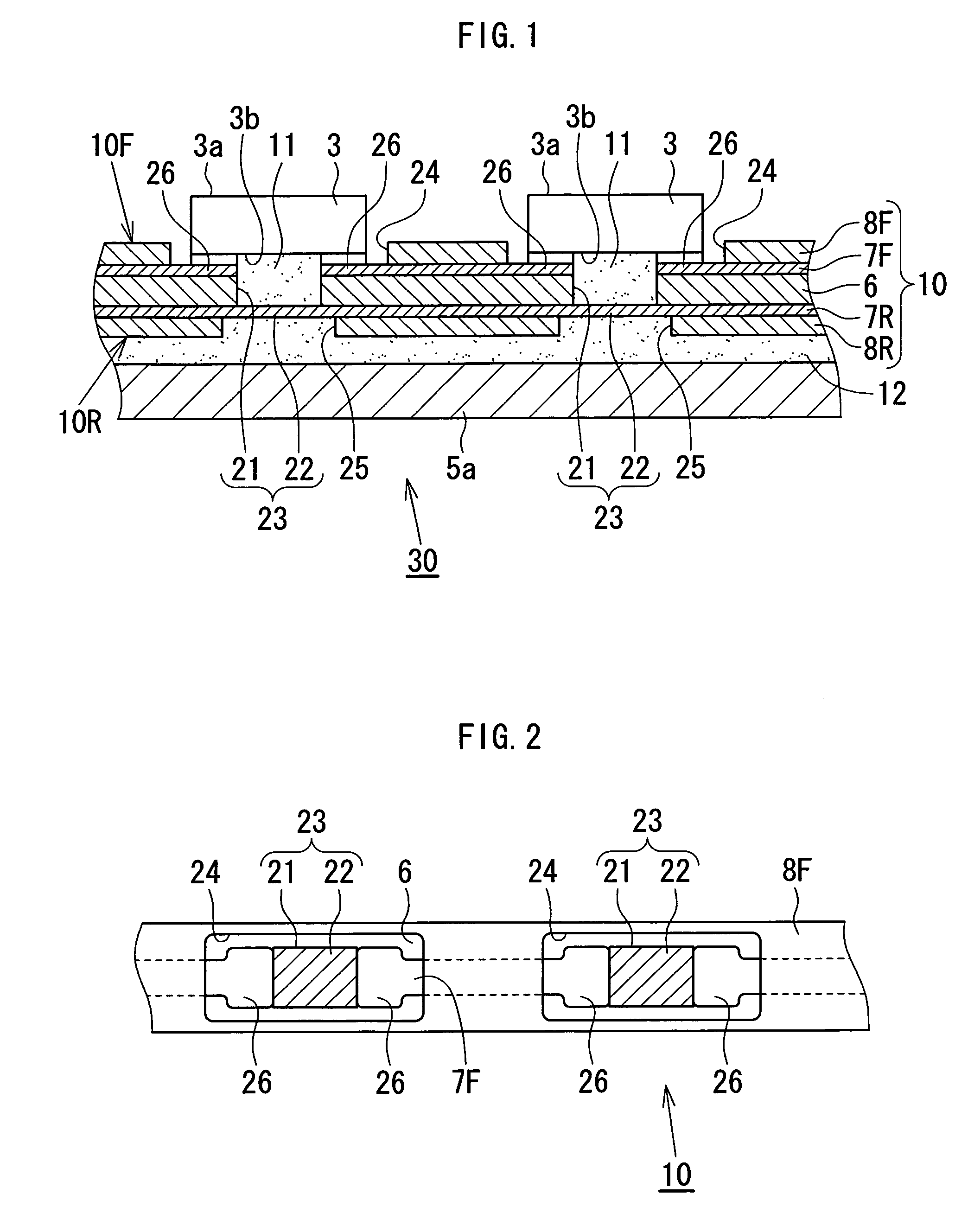
[0038]FIG. 1 is a sectional view illustrating an essential part of a light source portion 30 in the present invention, and FIG. 2 is a top view illustrating an essential part of a double-sided flexible print circuit board 10 used in the light source portion 30. In this embodiment, the double-sided flexible print circuit board (hereinafter referred to as FPC) 10 is provided with the base film 6 made of polyimide and the like, conductor patterns 7F, 7R formed by patterning copper foil and the like laminated on both principal faces of the base film 6, and cover films 8F, 8R made of polyimide and the like laminated so as to cover the respective conductor patterns 7F, 7R.

[0039]The conductor pattern 7F on the side of a surface 10F of the FPC 10 includes a land portion 26 on which a white LED, which is a point-like light source in this embodiment (hereinafter referred to as LED) 3 is mounted, the cover film 8F has an opening portion 24 exposing at least these land portions 26, and the LED ...

second embodiment

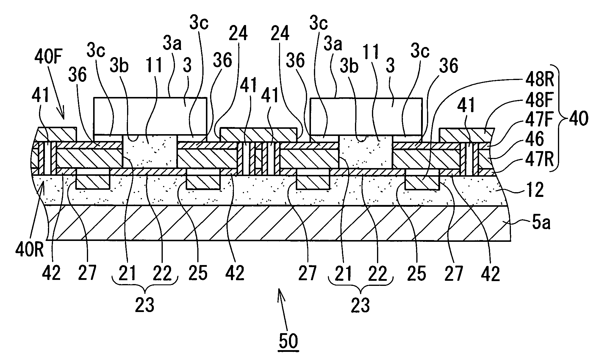
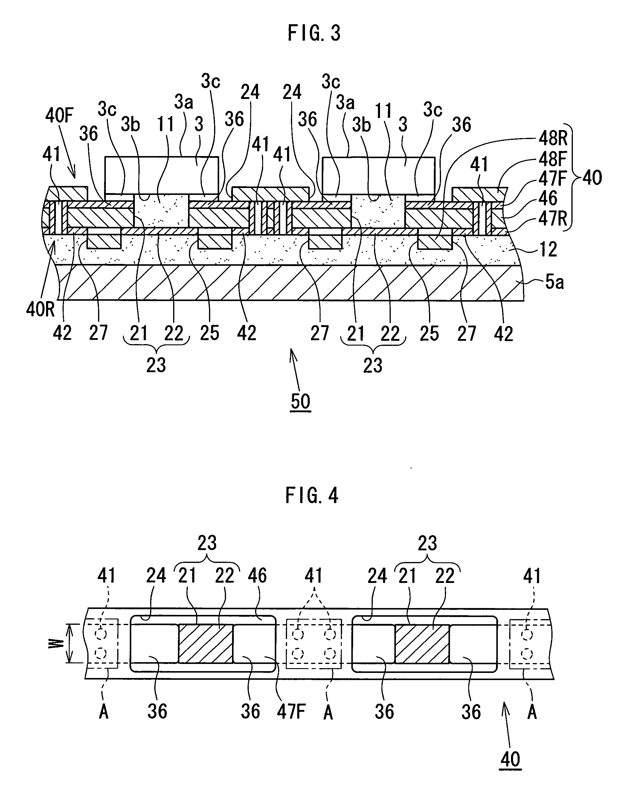
[0051]FIG. 3 is a sectional view illustrating an essential part of a light source portion 50 in the present invention, and FIG. 4 is a top view illustrating an essential part of an FPC 40 used in the light source portion 50. The FPC 40 in this embodiment has basic configuration similar to the FPC 10 and the light source portion 30 shown in FIGS. 1 and 2 and comprises a base film 46 made of polyimide and the like, conductor patterns 47F, 47R formed by patterning a copper foil and the like laminated on both principal faces of the base film 46, and a cover film 48F and (when necessary) a cover film 48R made of polyimide and the like laminated so as to cover the respective conductor pattern 47F, 47R, the heat conducting resin 11 is filled in a space constituted by the recess portion 23 provided in the FPC 40 and the mounting face 3b of the LED 3, a back face 40R side of the FPC 40 is fastened to the radiator plate 5a using the heat conducting tape 12, and a radiation path with high heat...


PUM


Abstract

A planar illumination device in which workability of a filling work of a heat conduction agent is improved and a heat generated from a point-like light source is efficiently radiated so as to achieve high brightness. In a planar illumination device 1 according to the present invention, a recess portion 23 is formed on a part of a face on which a point-like light source 3 is mounted in a double-sided flexible print circuit board 10, a bottom face 22 of the recess portion 23 is made of a conductor pattern 7R on the opposite side 10R of a side 10F on which the point-like light source is mounted in the double-sided flexible print circuit board 10, and a heat conducting resin 11 is filled in a space constituted by the recess portion 23 and the mounting face 3b of the point-like light source 3. The double-sided flexible print circuit board 10 is preferably mounted on a radiator plate 5a using a heat conducting tape 12.

Description

TECHNICAL FIELD[0001]The present invention relates to a side-light-type planar illumination device and particularly to a planar illumination device used as illuminating means of a liquid crystal display device.BACKGROUND ART[0002]As an auxiliary light source for a liquid crystal display device used for a cellular phone or the like, a side-light type planar illumination device in which a primary light source is arranged on a side end face of a light guide plate is mainly used (hereinafter the side end face on which the primary light source is arranged is also called an incoming-light face). As the primary light source of a side-light-type planar illumination device, a cold-cathode lamp has been used, but currently, a point-like light source such as a white LED (hereinafter referred to simply as LED) which is more excellent in handling, easier in size reduction and better in impact resistance than the cold-cathode lamp is used in many cases. Application fields of the planar illuminati...

Claims


Application Information

Patent Timeline
Patent Type & Authority Applications(United States)
IPC IPC(8): F21V7/04F21V29/00H01L33/62H01L33/64
CPCG02B6/0083H04M1/22H05K1/0206H05K1/189H05K2203/0191H05K3/4069H05K2201/0209H05K2201/0394H05K2201/10106H05K3/0061
Inventor OHNO, YASUO
Owner MINEBEA CO LTD
Why Eureka
Try Eureka