Thin-film type solar cell including by-pass diode and manufacturing method thereof

Inactive Publication Date: 2009-09-03
LG ELECTRONICS INC
View PDF10 Cites 5 Cited by
  • Summary
  • Abstract
  • Description
  • Claims
  • Application Information

AI Technical Summary

Benefits of technology

[0035]According to the present invention, a photovoltaic conversion apparatus having high photoelectric conversion efficiency can be manufactured.
[0036]Also, the photovoltaic conversion apparatus will contr

Problems solved by technology

The amorphous silicon based thin-film type solar cell has a disadvantage that the photoelectric conversion efficiency is relatively low as compared to the crystalline silicon based solar cell; however, it has much more room for improving the photoelectric conversion efficiency and it has an advantage of reducing manufacturing costs by increasing production rate through large and automated deposition equipment.
The problem in this structure is that since the solar cells are connected in series, the same amount of photocurrent should be generated in all the unit cells that are connected.
If the same amount of photocurrent is not generated in the respective unit cells, the current is limited by means of the cells generating less photocurrent s

Method used


Image

  • Thin-film type solar cell including by-pass diode and manufacturing method thereof
  • Thin-film type solar cell including by-pass diode and manufacturing method thereof
  • Thin-film type solar cell including by-pass diode and manufacturing method thereof

Examples


Example

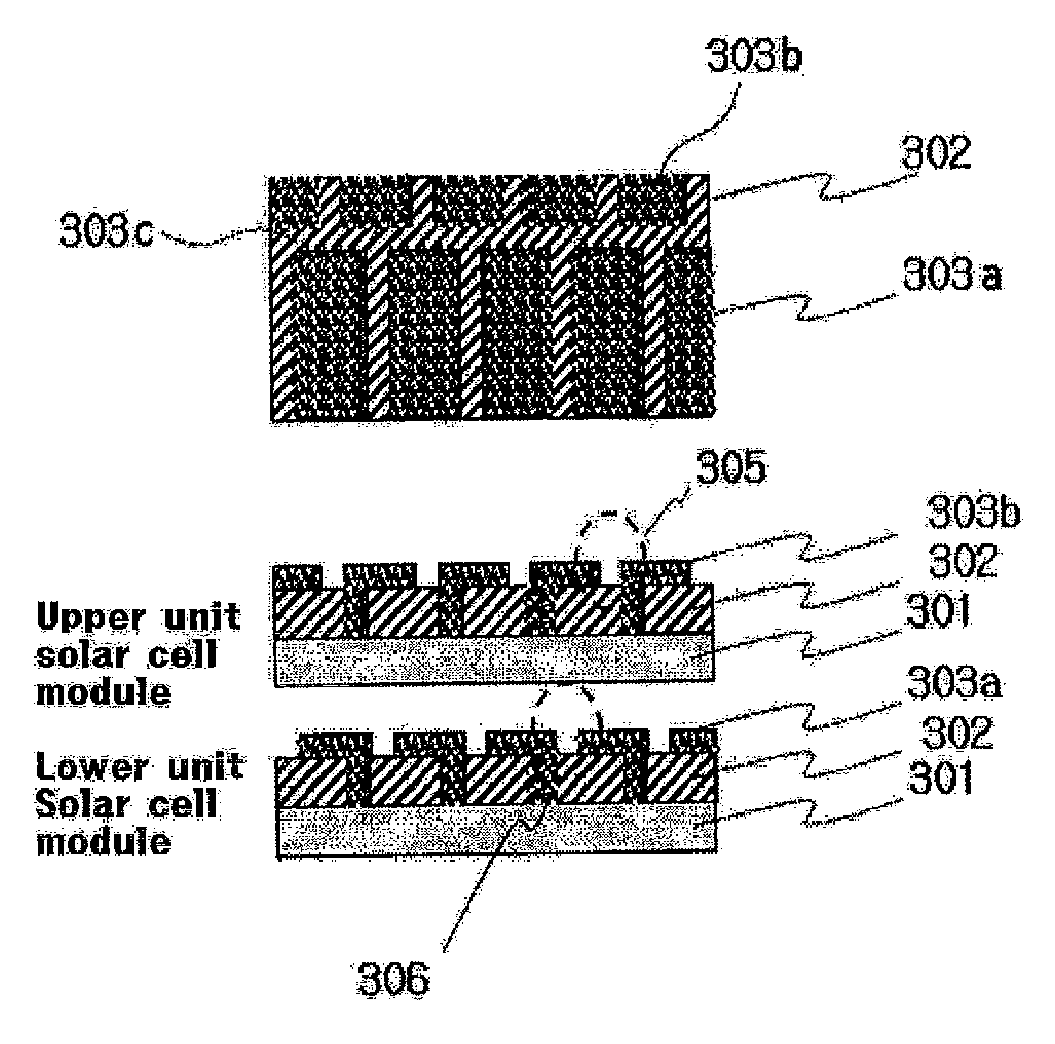
DESCRIPTION FOR KEY ELEMENTS IN THE DRAWINGS

[0042]301: Transparent substrate 302: Transparent conductive layer[0043]303: Photoelectric conversion layer 304: Backside electrode layer[0044]305: Upper photoelectric conversion layer pattern[0045]306: Lower photoelectric conversion layer pattern

BEST MODE

[0046]Hereinafter, the preferred embodiments of the present invention will be described with reference to the accompanying drawings. In indicating the reference numerals and signs for components throughout the following drawings, although the same components are shown in different drawings, they will be indicated by the same reference numerals and signs. A detailed description of known functions and configurations will be omitted so as not to obscure the subject of the present invention with unnecessary detail.

[0047]FIGS. 9 to 15 show a manufacturing process of a photovoltaic conversion apparatus including a by-pass diode according to one embodiment of the present invention, in particular...


PUM


Abstract

The present invention relates to a photovoltaic conversion apparatus including a by-pass diode and a manufacturing method thereof. The photovoltaic conversion apparatus of the present invention comprises at least one unit solar cell module configured of at least one unit solar cell; and a by-pass solar cell module including at least one solar cell electrically connected to the unit solar cell to by-pass current.
According to the present invention, a photovoltaic conversion apparatus having high photoelectric conversion efficiency can be manufactured. Also, the photovoltaic conversion apparatus will contribute to earths environmental conservation as the next clean energy source and can be directly applied to private facilities, public facilities, military facilities, etc., to create enormous economic value.

Description

TECHNICAL FIELD[0001]The present invention relates to a photovoltaic conversion apparatus including a by-pass diode and a manufacturing method thereof.[0002]More specifically, the present invention relates to a structure of a solar cell module including a solar cell including a by-pass diode and a manufacturing method thereof for overcoming problems of current limitation and hot spot generation due to the solar cell generating less photocurrent.BACKGROUND ART[0003]The outlook for fossil fuels that we are now been using is discouraging. In 2003, British Petroleum (BP), an oil refining company of England, predicted that considering the fossil fuels in recoverable deposits, crude oil may be in use for about 40 years, natural gas for about sixty two years and coal for about two hundred and sixteen years. However, since big consumers of energy, such as China and India have appeared, it is expected to be shorter than these predicted periods. Also, when considering soaring crude oil costs,...

Claims


Application Information

Patent Timeline
IPC IPC(8): H01L27/142H01L31/18H01L31/09
CPCH01L27/142H01L31/046Y02E10/50H01L31/044H01L31/047H01L31/06
Inventor EO, YOUNG-JOOKIM, HWA-NYEONAHN, SEH-WONLEE, HAE-SEOKLEE, HEON-MINYUN, JUNG-HEUMJI, KWANG-SUNKIM, BUM-SUNG
Owner LG ELECTRONICS INC
Why Eureka
Try Eureka