Chip package

a chip and package technology, applied in the field of chip packages, can solve the problems of deteriorating reliability and abnormal electrical connection of the chip package, and achieve the effects of enhancing the reliability of the chip package, and effectively preventing abnormal electrical connection

Inactive Publication Date: 2009-09-10
CHIPMOS TECH INC
View PDF11 Cites 21 Cited by
  • Summary
  • Abstract
  • Description
  • Claims
  • Application Information

AI Technical Summary

Benefits of technology

[0010]Accordingly, the present invention is directed to a chip package, wherein abnormal electrical connection caused by the overflowed adhesive is avoided and accordingly the reliability of the chip package can be enhanced.
[0019]In the present invention, the die pad has a blocking portion disposed on the top surface thereof so as to prevent the adhesive from contacting the grounding wires due to the overflowed adhesive. Accordingly, abnormal electrical connection can be effectively prevented, so that the reliability of a chip package can be enhanced. Moreover, in the present invention, the die pad may further have a groove to prevent abnormal electrical connection caused by overflow of the adhesive. Furthermore, openings may be formed on the bottom surface of the die pad and / or at one end of at least one lead adjacent to the die pad in order to increase the contact area between the die pad and the molding compound so that the leads would not peel off or delaminate from the die pad.

Problems solved by technology

However, the conductive paste in the conventional chip package may overflow and cause the chip package to have abnormal electrical connection and deteriorated reliability.
Besides, the conductive paste may be overheated by the pressure during the process so that the conductive particles in the conductive paste contact the grounding wires and accordingly electrically connect the conductive paste and the grounding wires.

Method used


Image

  • Chip package
  • Chip package
  • Chip package

Examples


Embodiment Construction

[0027]Reference will now be made in detail to the present preferred embodiments of the invention, examples of which are illustrated in the accompanying drawings. Wherever possible, the same reference numbers are used in the drawings and the description to refer to the same or like parts.

[0028]Several embodiments of the chip package structure provided by the present invention will be described below. However, these embodiments are not intended to limiting the scope of the present invention.

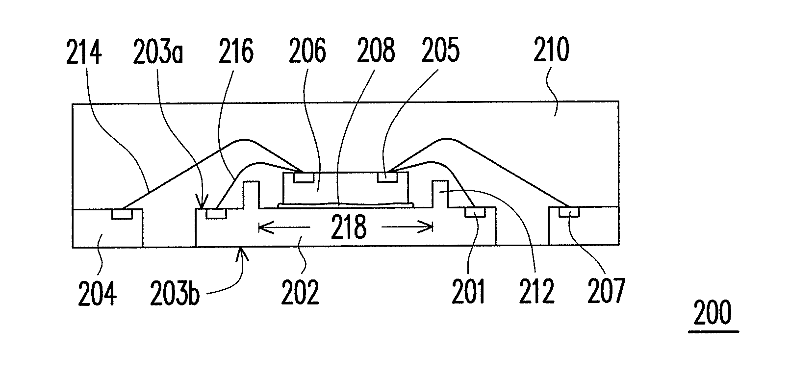
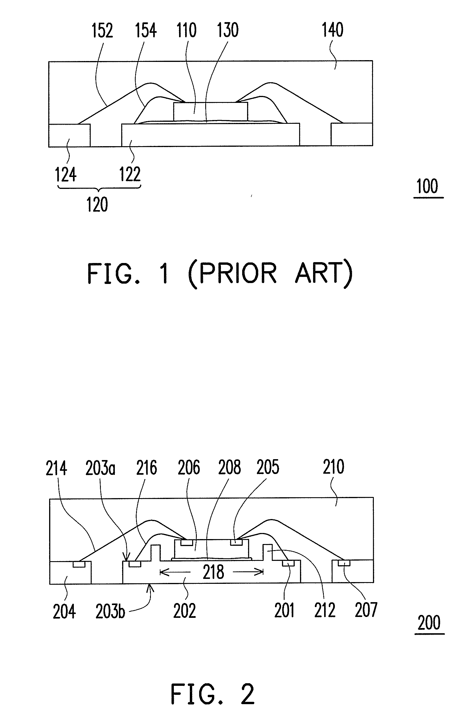
[0029]FIG. 2 is a cross-sectional diagram of a chip package according to an embodiment of the present invention.

[0030]As shown in FIG. 2, in the present embodiment, the chip package 200 includes a die pad 202, a plurality of leads 204, a chip 206, an adhesive 208, and a molding compound 210. The die pad 202 has a top surface 203a for supporting the chip and a bottom surface 203b opposite to the top surface 230a, and the leads 204 are disposed around the die pad 202. The chip 206 is disposed on the ...


PUM


Abstract

A chip package including a die pad, a plurality of leads, a chip, an adhesive, and a molding compound is provided. The die pad has a top surface and a bottom surface opposite to the top surface, wherein the die pad has a blocking portion disposed on the top surface, and the leads are disposed around the die pad. The chip is disposed on the top surface of the die pad surrounded by the blocking portion and is electrically connected to the leads. A top surface of the blocking portion is higher than the top surface of the die pad surrounded by the blocking portion. The adhesive is disposed between the chip and the die pad. The molding compound encapsulates the chip, a portion of the leads, and the die pad.

Description

CROSS-REFERENCE TO RELATED APPLICATION[0001]This application claims the priority benefit of Taiwan application serial no. 97108075, filed on Mar. 7, 2008. The entirety of the above-mentioned patent application is hereby incorporated by reference herein and made a part of specification.BACKGROUND OF THE INVENTION[0002]1. Field of the Invention[0003]The present invention generally relates to a chip package, and more particularly, to a chip package having excellent reliability.[0004]2. Description of Related Art[0005]In the semiconductor industry, the fabrication of integrated circuits (IC) can be divided into three phases: IC design, IC fabrication process, and IC packaging.[0006]Regarding IC packaging, a chip is fabricated through wafer fabrication, circuit design, photolithography and etching processes, and wafer dicing, etc. Each chip is electrically connected to a substrate through a bonding pad on the chip, and the chip is encapsulated by a molding compound to form a chip package...

Claims


Application Information

Patent Timeline
Patent Type & Authority Applications(United States)
IPC IPC(8): H01L23/495
CPCH01L23/3107H01L2224/32257H01L24/32H01L2224/27013H01L2224/32245H01L2224/48091H01L2224/48247H01L2224/48257H01L2224/73265H01L2224/83051H01L2224/83385H01L2924/01047H01L2924/01079H01L2924/01082H01L23/49503H01L2224/45144H01L24/48H01L2924/01005H01L2924/01033H01L2924/01074H01L2924/00014H01L2924/00012H01L2924/00H01L24/45H01L24/73H01L2924/14H01L2924/181H01L2224/05599
Inventor HOU, PO-KAISHIH, CHI-JIN
Owner CHIPMOS TECH INC
Why Eureka
Try Eureka