

Emission device, surface light source device and display
- Summary
- Abstract
- Description
- Claims
- Application Information
AI Technical Summary
Benefits of technology
Problems solved by technology
Method used
Image

Examples
Embodiment Construction
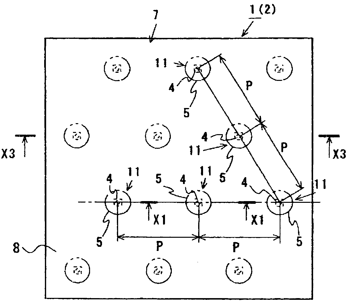
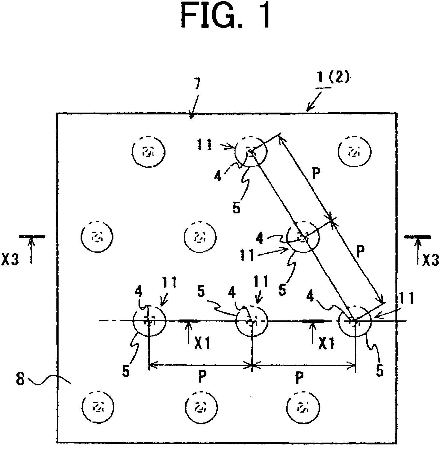
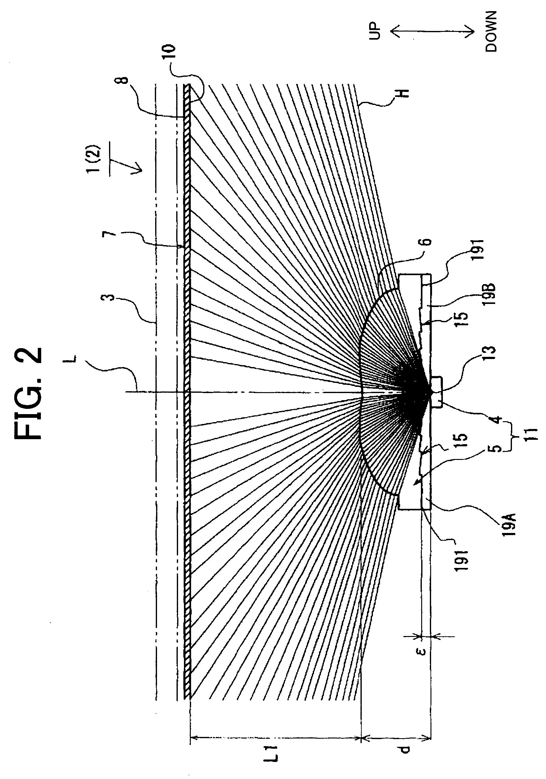
[0244]According to the embodiment, a greater part of the light emitted from emission element 4 enters into light flux control member 5, being emitted from light control emission face 6. Some of the light emitted from emission element 4 enters into light flux control member 5 via in-groove-recess portions 15a to 15d formed at groove bottoms 191 of ventilation grooves 19A, 19B. Such light H becomes inner-propagation light which is not deflected as to come nearer to optical axis L by refraction on incidence to in-groove-recess portions 15.
[0245]As a result, light H via in-groove-recess portions 15 is not emitted from light control emission face 6, or, if some emission involved, it occurs in the vicinity of the outermost periphery of light control emission face 6. This prevents ring-like, pint-like or line-like locally bright part from appearing, with the result that illumination light is kept high. Emission from light control emission face 6 is broadly and smoothly diverged, providing ...
PUM
 Abstract
Description
Claims
Application Information