Silicon based light emitting diode

Active Publication Date: 2009-10-01
ELECTRONICS & TELECOMM RES INST
View PDF0 Cites 19 Cited by
  • Summary
  • Abstract
  • Description
  • Claims
  • Application Information

AI Technical Summary

Benefits of technology

[0012]The silicon-based LED uses only the n-type doping layer to form a reflective layer on both surfaces of the active la

Problems solved by technology

However, current silicon-based LEDs are not widely used in commercial applications because of their low emission efficiency and wide emission spectrum.
However, in a silicon-based LED using silicon nano-size dots, there is a problem indirectly doping a DBR, because the DBR is typically composed

Method used


Image

  • Silicon based light emitting diode
  • Silicon based light emitting diode
  • Silicon based light emitting diode

Examples


Embodiment Construction

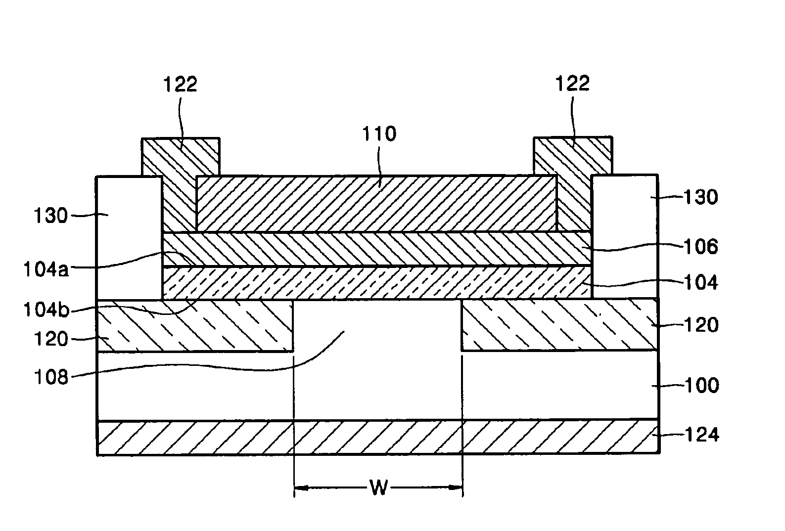
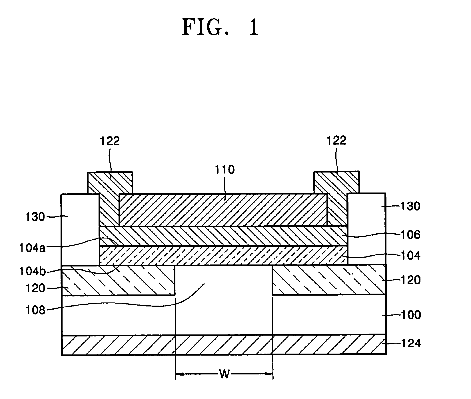
[0017]To improve the performance of a light emitting diode (LED), it is very important to effectively arrange an active layer for generating light, a doped layer in which carriers are injected, and a reflective layer for effectively reflecting light. In particular, the effective arrangement of a doping layer and an active layer is important in a silicon-based LED using silicon nano-size dots offering low self-emission.

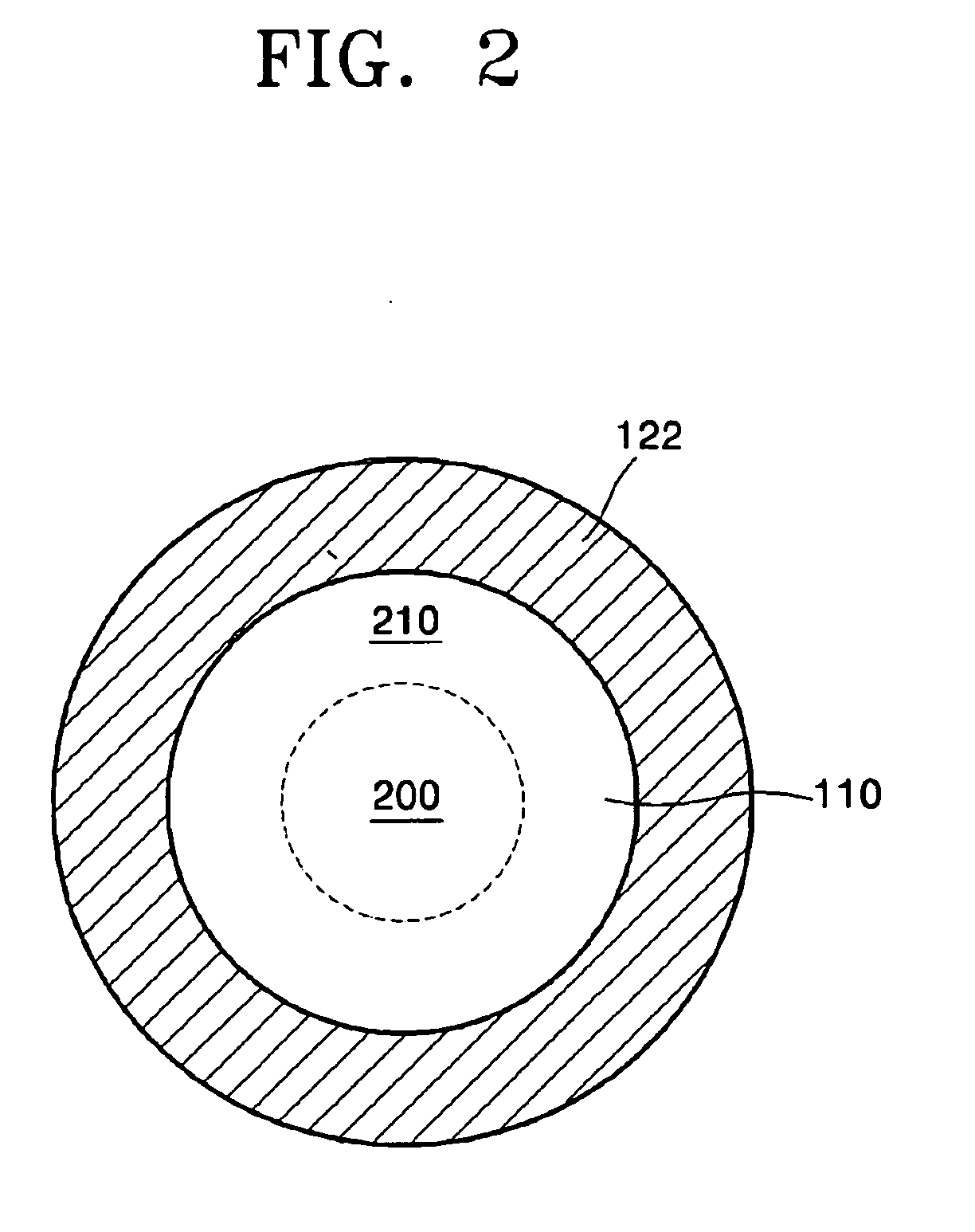
[0018]Referring to FIGS. 1 and 2, a silicon-based light emitting diode (LED) according to an embodiment of the present invention includes a substrate 100, for example, p-type silicon substrate, and an active layer 104 that is formed on the substrate 100 and has a first surface 104a and a second surface 104b opposite the first surface 104a. The substrate 100 has a p-type mesa structure 108. The active layer 104 is formed of crystalline or amorphous silicon nano-size dots, and may have a thickness of 10 nm to 100 μm.

[0019]A first reflective layer 110 faces the first surf...


PUM


Abstract

Provided is a highly efficient silicon-based light emitting diode (LED) including a Distributed Bragg Reflector (DBR), an n-type doping layer, and a p-type substrate structure. The silicon-based LED includes: a substrate having a p-type mesa substrate structure; an active layer that is formed on the substrate and has a first surface and a second surface opposite the first surface; a first reflective layer facing the first surface of the active layer; a second reflective layer that is located on either side of the p-type substrate structure and faces the second surface of the active layer; an n-type doping layer sandwiched between the active layer and the first reflective layer; a first electrode electrically connected to the n-type doping layer; and a second electrode electrically connected to the p-type substrate structure.

Description

CROSS-REFERENCE TO RELATED PATENT APPLICATION[0001]This application claims the benefit of Korean Patent Application No. 10-2004-0102956, filed on 8 Dec. 2004 and Korean Patent Application No. 10-2005-0037623, filed on 4 May 2005 in the Korean Intellectual Property Office, the disclosures of which are incorporated herein in their entirety by reference.BACKGROUND OF THE INVENTION[0002]1. Field of the Invention[0003]The present invention relates to a method of manufacturing a semiconductor device, and more particularly, to a silicon-based light emitting diode (LED) including a distributed Bragg reflector (DBR).[0004]2. Description of the Related Art[0005]Much research has been conducted into silicon-based LEDs using silicon nano-size dots, because they are easily compatible with silicon-based photoelectronic devices and have low manufacturing costs. However, current silicon-based LEDs are not widely used in commercial applications because of their low emission efficiency and wide emiss...

Claims


Application Information

Patent Timeline
IPC IPC(8): H01L33/00H01L33/06H01L33/10H01L33/14H01L33/16H01L33/34
CPCH01L33/34H01L33/465H01L33/38
Inventor KIM, TAE-YOUBPARK, NAE-MANKIM, KYUNG-HYUNSUNG, GUN-YONG
Owner ELECTRONICS & TELECOMM RES INST
Why Eureka
Try Eureka