Semiconductor device

Inactive Publication Date: 2009-10-08
RENESAS ELECTRONICS CORP
View PDF54 Cites 10 Cited by
  • Summary
  • Abstract
  • Description
  • Claims
  • Application Information

AI Technical Summary

Benefits of technology

[0021]In contrast, according to the present invention, the direction in which electrons flow through the first electrical fuse and the second electrical fuse is the same, and therefore the cut state is the same between the first electrical fuse and the second electrical fuse, and the ease of cutting can also be approximately the same between the first electrical fuse and the second electrical fuse.
[0022]As a result, inconsistency in the resistance value can be prevented between a state where the first electrical fuse is cut and a s

Problems solved by technology

The technology described in Japanese Laid-Open Patent Publication 2005-57186, however, has the following problems.
Thus, the cut state may be different between the fused via portions 903 and 904, and in addition the ease of cutting is different, and therefore there may be inconsistency in the resistance value after the fuses are cut.
As described abov

Method used


Image

  • Semiconductor device
  • Semiconductor device
  • Semiconductor device

Examples


first embodiment

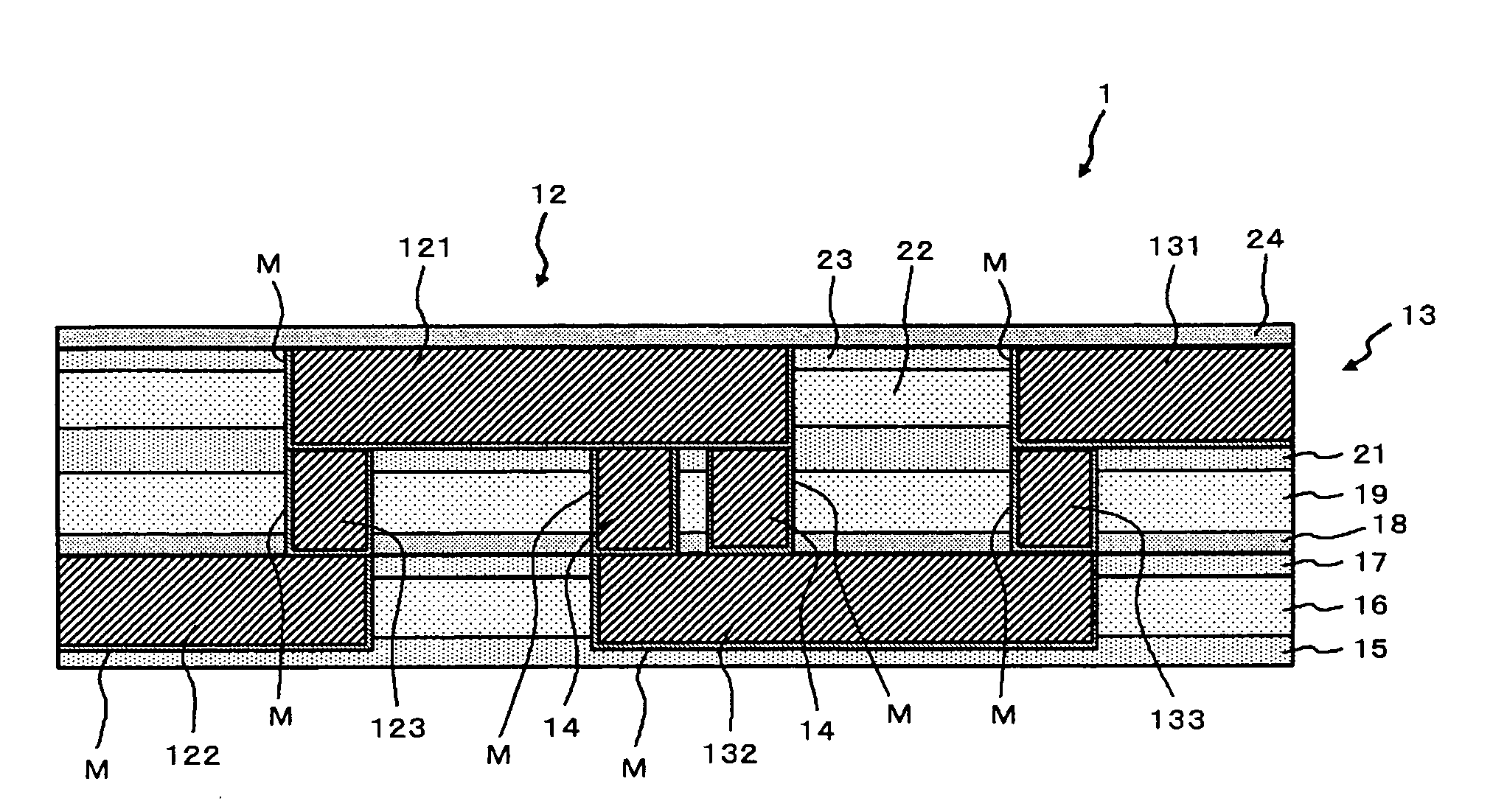
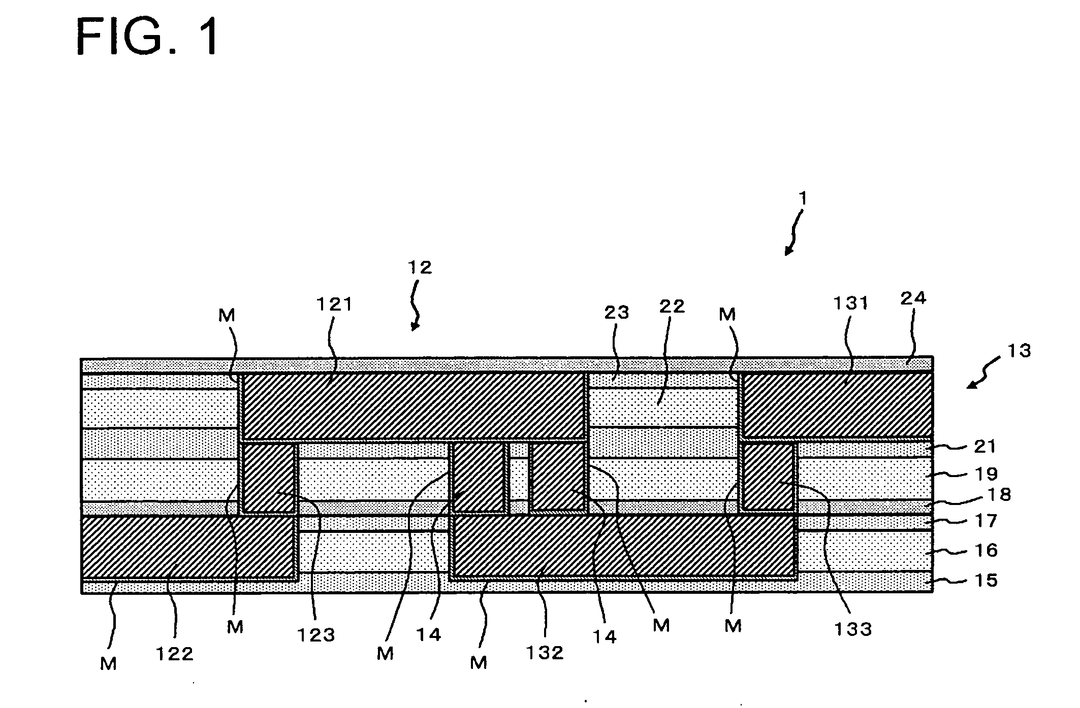
[0034]FIG. 1 is a cross sectional diagram showing a semiconductor device 1 according to the present embodiment.

[0035]The semiconductor device 1 according to the present embodiment is provided with a substrate (for example a semiconductor substrate) (not shown), and a first electrical fuse 12 and a second electrical fuse 13, which are provided on the semiconductor substrate.

[0036]The first electrical fuse 12 has a first upper layer wire 121 and a first lower layer wire 122 formed in different wire layers, and a via 123 for connecting the first upper layer wire 121 to the first lower layer wire 122.

[0037]The second electrical fuse 13 has a second upper layer wire 131 and a second lower layer wire 132 formed in different wire layers, and a via 133 for connecting the second upper layer wire 131 to the second lower layer wire 132.

[0038]Furthermore, the semiconductor device 1 according to the present embodiment has a connection portion 14 for connecting the first upper layer wire 121 of t...

second embodiment

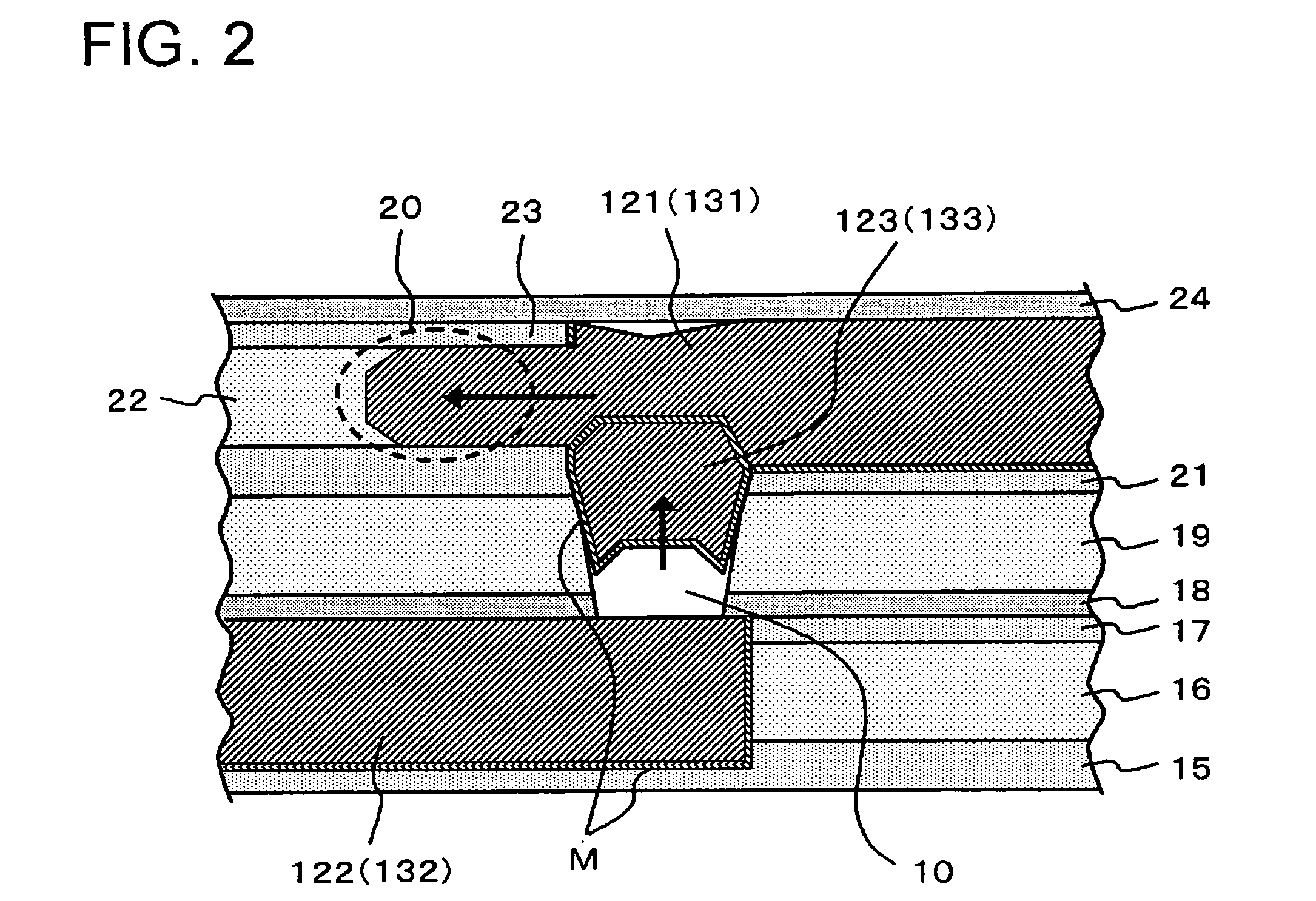
[0099]The semiconductor device 2 according to the present embodiment is described in reference to FIG. 3.

[0100]The first electrical fuse 12 and the second electrical fuse 13 are formed in the same wire layer in the above described embodiment.

[0101]In contrast, in the present embodiment, the first electrical fuse 12 and the second electrical fuse 13 are formed in different wire layers.

[0102]Furthermore, the connection portions 14 are made of vias in the above described embodiment, while the connection portions are wires 34 for connecting the first upper layer wire 121 of the first electrical fuse 12 to the second lower layer wire 132 of the second electrical fuse 13, which is formed in the same wire layer as the first upper layer wire 121 and the second lower layer wire 132.

[0103]The rest is the same as in the above described embodiment.

[0104]In the following, the semiconductor device 2 according to the present embodiment is described in detail.

[0105]In the present embodiment, the se...


PUM


Abstract

A semiconductor device 1 has a semiconductor substrate and a first electrical fuse 12 and a second electrical fuse 13, which are provided on the semiconductor substrate. The first electrical fuse 12 has a first upper layer wire 121 and a first lower layer wire 122 formed in different wire layers, and a via 123 for connecting the first upper layer wire 121 to the first lower layer wire 122. The second electrical fuse 13 has a second upper layer wire 131 and a second lower layer wire 132 formed in different wire layers, and a via 133 for connecting the second upper layer wire 131 to the second lower layer wire 132. The semiconductor device 1 has a connection portion 14 for connecting the above described first upper layer wire 121 of the first electrical fuse 12 to the second lower layer wire 132 of the second electrical fuse 13. The connection portion 14 connects the first electrical fuse 12 and the second electrical fuse 13 in series.

Description

[0001]This application is based on Japanese patent application NO. 2008-096918, the content of which is incorporated hereinto by reference.BACKGROUND[0002]1. Technical Field[0003]The present invention relates to a semiconductor device provided with an electrical fuse.[0004]2. Related Art[0005]Conventional semiconductor devices are known where a fuse is mounted so that a process can be carried out, for example the fuse can be cut to adjust the resistance value or separate a defective element, which is thus replaced with a normal element.[0006]In order to provide a highly reliable semiconductor device where such a process can be carried out, it is necessary for the fuse to be cut without failure. Therefore, the fuse disclosed in Japanese Laid-Open Patent Publication 2005-57186 has been proposed.[0007]As shown in FIG. 5, Japanese Laid-Open Patent Publication 2005-57186 discloses a fuse having a current flow-in terminal 902, a current flow-out terminal 901, a pair of fused via portions ...

Claims


Application Information

Patent Timeline
IPC IPC(8): H01H85/04
CPCH01L23/5256H01L23/5329H01L23/53295H01L2924/0002H01L2924/00
Inventor TSUDA, HIROSHI
Owner RENESAS ELECTRONICS CORP
Why Eureka
Try Eureka