Semiconductor Package, Method for Manufacturing the Same, Semiconductor Module, and Electronic Device

a technology of semiconductor modules and semiconductor modules, applied in the direction of semiconductor devices, semiconductor/solid-state device details, electrical apparatus, etc., can solve the problems of not being able to fully meet the needs of conventional arrangements and the worsening of achieve the effect of high precision and worsening the function of the camera

Inactive Publication Date: 2009-10-15
SHARP KK
View PDF9 Cites 91 Cited by
  • Summary
  • Abstract
  • Description
  • Claims
  • Application Information

AI Technical Summary

Benefits of technology

[0013]Not only downsizing but also alignment between a semiconductor chip and a lens member are important in the camera modules as above. Misalignment therebetween worsens the function of a camera. Therefore it is necessary for them to be aligned with high precision.
[0022]The present invention has been attained in view of the above problems, and an object of the present invention is to realize a semiconductor module that allows for its downsizing and highly precise alignment between a semiconductor package constituting the semiconductor module and the mounting component. Another object of the present invention is to provide a method for manufacturing a semiconductor package used suitably in such a semiconductor module and the use of the semiconductor module.
[0025]Furthermore, according to the above arrangement, the step is formed around the perimeter of the resin sealing member. By attaching the mounting component which fits in this step to the semiconductor package, it is possible to form a semiconductor module that allows for highly precise alignment lengthwise and crosswise. That is, the semiconductor package of the present invention can be applied suitably to such a semiconductor module.
[0026]Thus, a semiconductor package according to the present invention is arranged such that the step is formed around the perimeter of the surface of the resin sealing member. This makes it possible to realize a super-small semiconductor package and a semiconductor package which is suitable for the semiconductor module which allows for highly precise alignment lengthwise and crosswise by attaching the mounting component which fits in this step to the semiconductor package.
[0028]According to the above method, the step forming step is included. This makes it possible to manufacture a semiconductor package that is suitable for the semiconductor module as described previously, i.e. the semiconductor module that allows for highly precise alignment lengthwise and crosswise.

Problems solved by technology

Misalignment therebetween worsens the function of a camera.
However, the conventional arrangements cannot fully meet the needs for downsizing of a camera module and highly precise alignment between the semiconductor chip and the lens member.

Method used


Image

  • Semiconductor Package, Method for Manufacturing the Same, Semiconductor Module, and Electronic Device
  • Semiconductor Package, Method for Manufacturing the Same, Semiconductor Module, and Electronic Device
  • Semiconductor Package, Method for Manufacturing the Same, Semiconductor Module, and Electronic Device

Examples


Embodiment Construction

[0042]One embodiment of the present invention is described below with reference to FIG. 1 through FIG. 5.

[0043](1) Camera Module in Accordance with the Present Invention

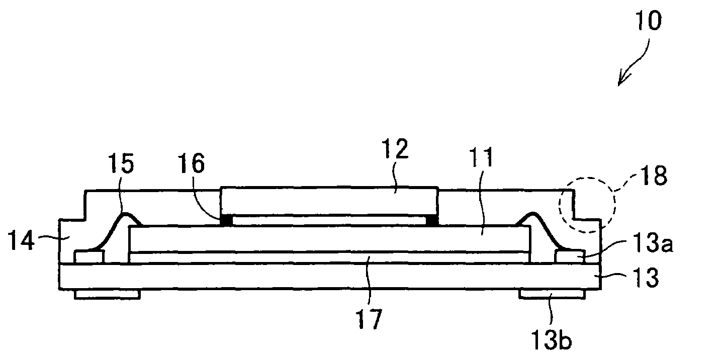
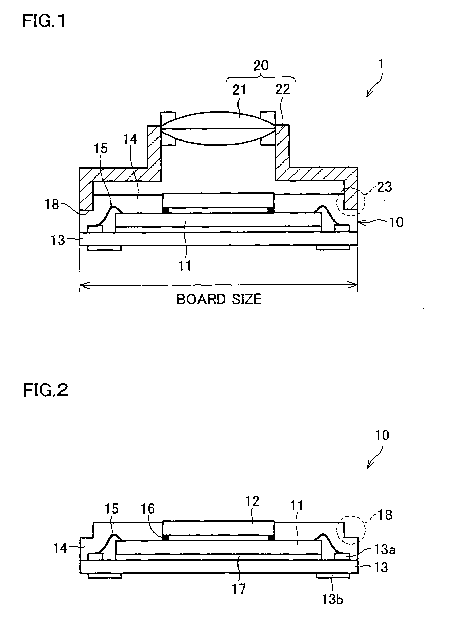
[0044]FIG. 1 shows a cross-sectional view of a camera module 1 in accordance with the present embodiment. The camera module 1 has the structure in which a lens member 20 is integrally attached to a semiconductor package 10.

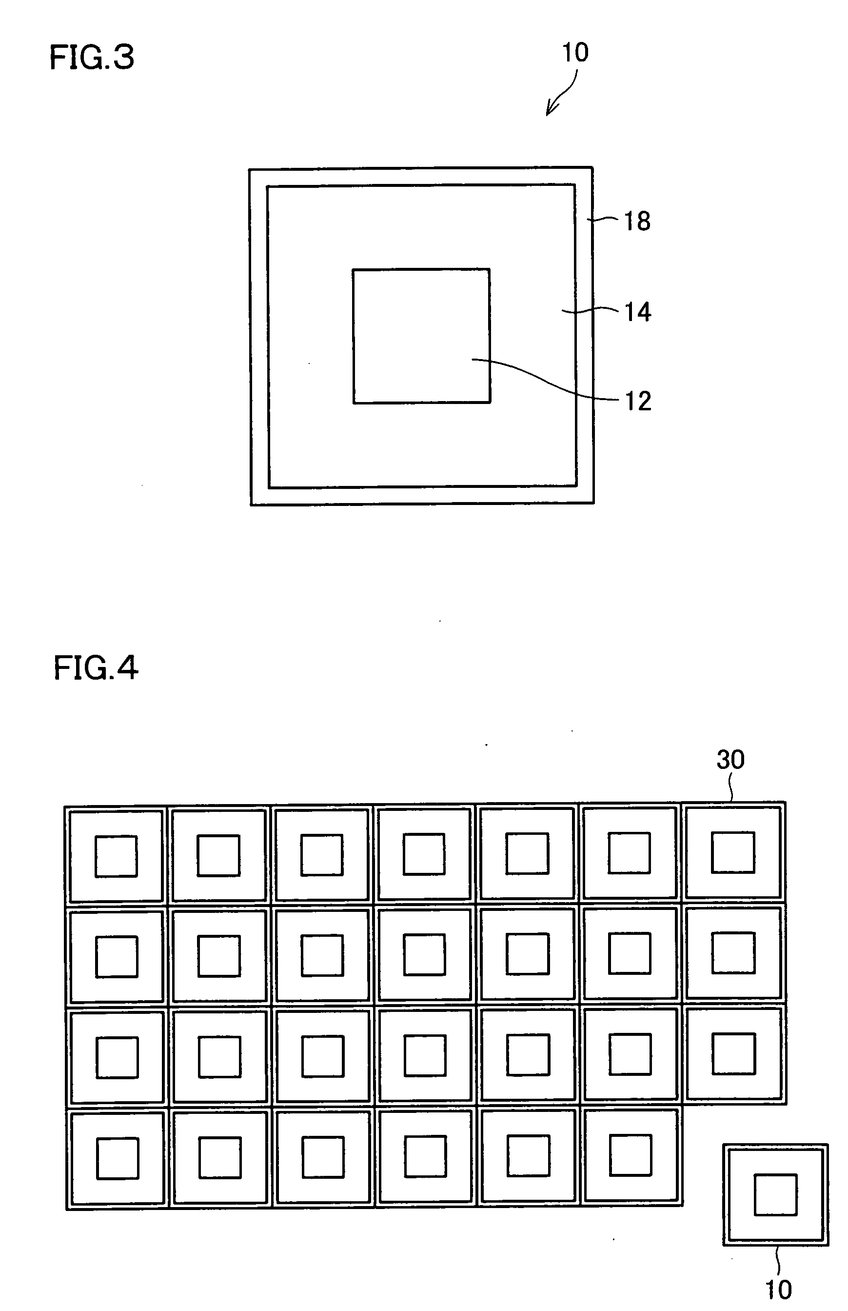
[0045]FIG. 2 is a cross-sectional view of the semiconductor package 10 and FIG. 3 is a top view of the semiconductor package 10. The semiconductor package 10 has the structure in which an image sensor 11 is mounted on a print wiring board 13 (hereinafter referred to as “the wiring board”) 13.

[0046]The wiring board 13 has wiring pattern formed thereon. The wiring board 13 has a wire bond terminal 13a provided on its surface where the image sensor 11 is mounted, and has an external connection electrode 13b provided on the other side (backside). The wire bond terminal 13a and the external connection e...


PUM


Abstract

In a camera module (1) of the present invention, a lens member (20) is attached to a semiconductor package (10). The semiconductor package (10) includes: an image sensor (11) mounted on a wiring board (13); and a wire 15 through which the wiring board (13) is electrically connected to the image sensor (11). The image sensor (11) and the wire 15 are sealed with mold resin (14). A step (18) is formed around the perimeter of the surface of the mold resin (14), and the semiconductor package (10) and the lens member (20) are joined by fitting the step (18) and a projection (23) of a lens holder (22). With this arrangement, it is possible to realize a small semiconductor module that allows for highly precise alignment between the semiconductor package and a mounting component to which the semiconductor package is joined.

Description

TECHNICAL FIELD[0001]The present invention relates to a semiconductor package, a method for manufacturing the same, a semiconductor module including the semiconductor package, and an electronic device including the semiconductor module.BACKGROUND ART[0002]In recent years, electronic cameras including an image pickup element have been used for various electronic devices such as mobile phones, personal digital assistants, personal computers and digital still cameras. At present there have been demands for downsizing and cost reduction on these electronic cameras. Therefore there has been increasing use of a downsized camera module into which an image sensor (semiconductor chip) and a lens are integrated (packaged).[0003]Thus, demands for downsizing of a camera module have been increasing. However, the size of the area which is used for alignment with an image sensor and a lens holder supporting a lens has a great influence on a module size these days.[0004]For example, downsized camer...

Claims


Application Information

Patent Timeline
Patent Type & Authority Applications(United States)
IPC IPC(8): H01L31/04H01L23/02H01L21/00
CPCH01L24/97H01L2224/48227H01L27/14625H01L2224/48091H01L2224/97H01L2924/01015H01L2924/01033H01L2924/01047H01L2924/01078H01L2924/01082H01L2924/14H01L2924/3025H01L27/14618H01L2924/014H01L2924/01006H01L2924/01005H01L2924/00014H01L2224/85H01L2224/83H01L2924/1815H01L2924/181H01L2924/00H01L23/28H01L27/14
Inventor ISHIKAWA, KAZUHIRONISHIDA, KATSUITSUFUJITA, KAZUYANAKAHASHI, TAKAHIRO
Owner SHARP KK
Why Eureka
Try Eureka