[0011]An object of the invention is to solve the problems with the conventional techniques described above and to provide an optical display device manufacturing method capable of reducing the total cost and ensuring bonding accuracy and high-speed bonding. Another object of the invention is to provide a material roll suitable for use in such a manufacturing method.
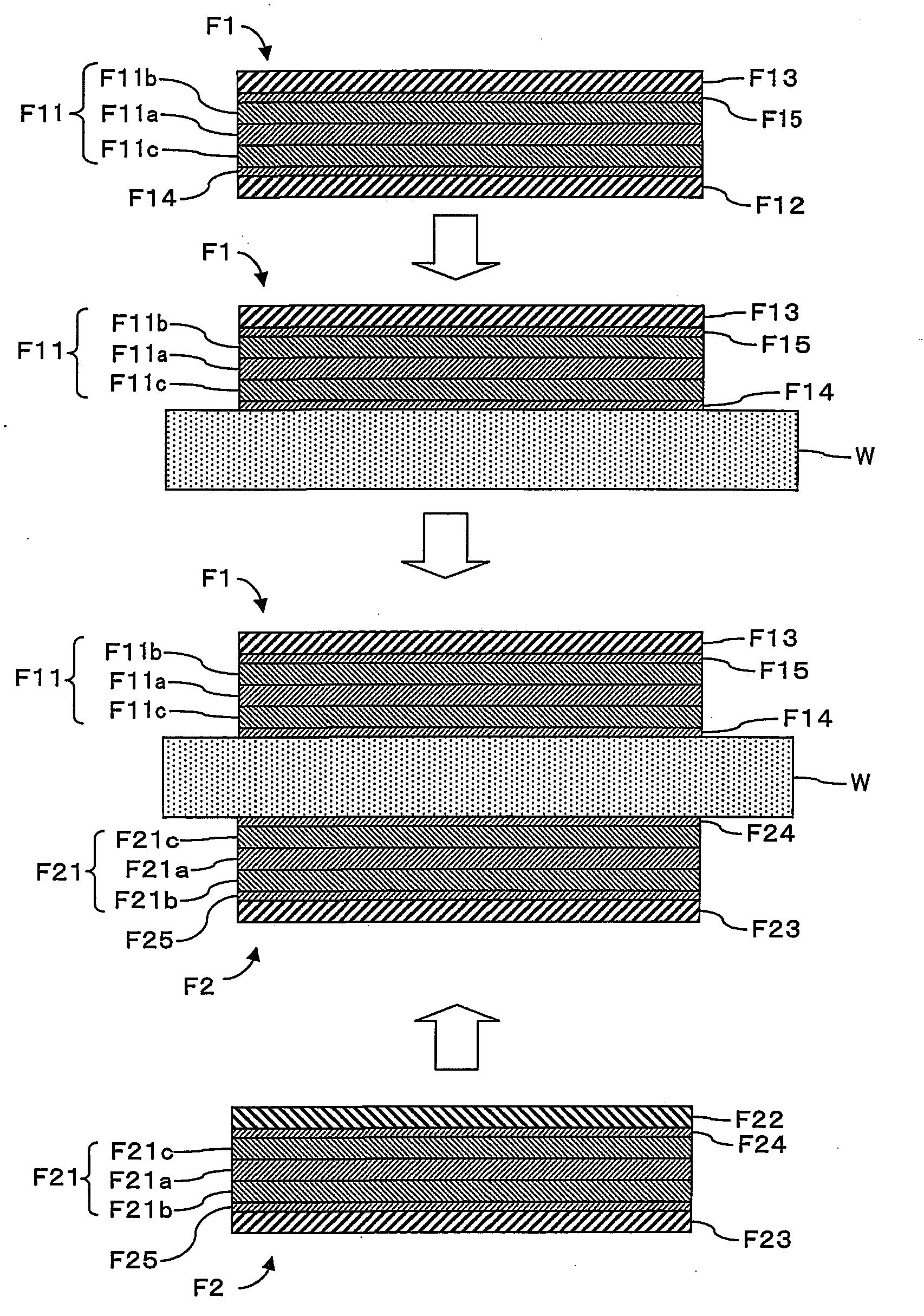
[0013]The optical display device manufacturing method of the invention employs a roll of a long sheet material that includes an optical film, a pressure-sensitive adhesive layer and a release film laminated in this order and has undergone a slitting process in a direction parallel or at a constant angle to the absorption axis of the polarizing plate so that it has a width corresponding to the short or long side of the optical display unit. According to the method of the invention, therefore, the optical film only has to be cut in the width direction. Moreover, a remaining portion in the width direction can be used, because the roll of the long sheet material is manufactured from a wide material roll by slitting it with the width corresponding to the width of the short side or long side of the LCD product. Namely, it becomes possible to be able to use the edge portions as a product of this invention, which are disposed in the ordinal process, because the slit can be done again or at the same time according to size of LCD panel with the same width as the edge portion or smaller, so that the area yield of the overall film cam be improved greatly. Moreover, the release film can also be used as a carrier so that the process of bonding the optical film to a liquid crystal cell or the like can be continuously performed, while the optical film is transported, which allows a continuous production flow from inspection to bonding. Therefore, when continuous production is performed according to the manufacturing method, there becomes advantageous in contrast to conventional methods with regard to its total cost and manufacturing amount.
[0015]The optical display device manufacturing method of the invention also employs the roll of the long sheet material having undergone a slitting process in a direction parallel or at a constant angle to the absorption axis of the polarizing plate so that it has a width corresponding to the short or long side of the optical display unit. According to the method of the invention, therefore, the optical film only has to be cut in the width direction, so that the loss L can be reduced. In addition, edge portions, which would otherwise be discarded in conventional processes, can be used depending on the size of a liquid crystal cell or the like. In the method of the invention, the release film can also be used as a carrier so that the process of bonding the optical film to a liquid crystal cell or the like can be continuously performed, while the optical film is transported, which allows a continuous production flow from cutting to bonding. In this process, the roll used already has defect information identifying the defect positions so that the step of detecting defects can be omitted from a series of steps, which can further improve the manufacturing speed. Therefore, when continuous production is performed according to the manufacturing method of the invention, a reduction in cost and an improvement in manufacturing speed can be accelerated as more products are manufactured, in contrast to conventional methods.
[0017]The above method employs a set of rolls including a roll having undergone a slitting process so that it has a width corresponding to the short side of the optical display unit and another roll having undergone a slitting process so that it has a width corresponding to the long side of the optical display unit. According to this method, therefore, optical films of sizes corresponding to the short and long sides of the optical display unit can be obtained, respectively, simply by cutting them into lengths corresponding to the long and short sides, respectively. At the same time, one of the optical films has an absorption axis parallel or at a constant angle to the long side of the optical display unit, and the other has an absorption axis parallel or at a constant angle to the short side. Therefore, the absorption axes of the optical films can be made orthogonal to each other with high accuracy simply by bonding them to the upper and lower sides of the optical display unit, respectively.
[0018]The optical display unit is preferably a VA or IPS mode liquid crystal panel. Particularly when the optical display unit includes a VA or IPS mode liquid crystal panel, which has been used for large screen TVs or the like in recent years, the polarizing plates of the first and second optical films should be so placed that their absorption axes can be orthogonal to each other and can be parallel to the directions of the long and short sides of the optical display unit Therefore, the first and second rolled materials each having undergone a slitting process in a direction parallel to the absorption axis only have to be unwound and cut in the width direction, so that a high production rate can be achieved. Particularly in the case of IPS mode, since the liquid crystal director is usually parallel or orthogonal to the side of LC panel in non-electric field, it is very important for obtaining a black display to bond a polarizing plate so that the director is parallel to an absorption axis of the polarizing plate. If this angle shifts, the influence of the retardation in the liquid crystal panel will arise, an optical leakage is induced, and the fall of a contrast ratio is caused. Since in this invention the direction of the absorption axis of a polarizing plate is parallel to the long side or the short side of the optical film and is bonded parallel to the short side or the long side of a liquid crystal panel, the direction of the liquid crystal director of LCD and the direction of the absorption axis can be coincided easily.
[0021]The material roll of the invention includes a roll of a long sheet material including the optical film, a pressure-sensitive adhesive layer and a release film laminated in this order and having undergone a slitting process in a direction parallel or at a constant angle to the absorption axis of the polarizing plate so that it has a width corresponding to the short or long side of the optical display unit. When the roll of the invention is used, therefore, the optical film only has to be cut in the width direction. Moreover, a remaining portion in the width direction can be used, because the roll of the long sheet material is manufactured from a wide material roll by slitting it with the width corresponding to the width of the short side or long side of the LCD product. Namely, it becomes possible to be able to use the edge portions as a product of this invention, which are disposed in the ordinal process, because the slit can be done again or at the same time according to size of LCD panel with the same width as the edge portion or smaller, so that the area yield of the overall film cam be improved greatly. In addition, the release film can be used as a carrier so that the process of bonding the optical film to a liquid crystal cell can be continuously performed, while the optical film is transported, which allows a continuous production flow from inspection to bonding. Therefore, when continuous production is performed according to the manufacturing method, there becomes advantageous in contrast to conventional methods with regard to its total cost and manufacturing amount.

