
Switching regulator

Active Publication Date: 2009-12-10
NISSHINBO MICRO DEVICES INC
View PDF7 Cites 68 Cited by
  • Summary
  • Abstract
  • Description
  • Claims
  • Application Information

AI Technical Summary

Benefits of technology

[0020]The present invention provides a switching regulator in which one or more of the above-described disadvantages are eliminated.
[0021]A preferred embodiment of the present invention provides a switching regulator for implementing control by performing slope compensation, whereby the switching regulator has two feedback paths for the output voltage and the inductor current. The switching regulator is capable of maintaining high efficiency even under light load conditions in which the load requires low current, without the need of adding a circuit for controlling the peak current of the inductor current. Furthermore, the switching regulator is capable of reducing ripples of the output voltage.
[0024]According to one embodiment of the present invention, a switching regulator is provided, which has two feedback paths. A slope voltage having a slope that is inversely proportional to a slope of the inductor current detected while a first switch is turned off and in a cutoff status. Therefore, the switching regulator is capable of maintaining high efficiency even under light load conditions in which the load requires low current, without the need of adding a circuit for controlling the peak current of the inductor current. Furthermore, the switching regulator is capable of reducing ripples of the output voltage.

Problems solved by technology

The loss generated in accordance with the operation of the switching regulator accounts for a high percentage of the total power loss.
Accordingly, the efficiency of the switching regulator declines when the load is light.
However, in the switching regulator for performing PWM control with the use of two feedback paths for the output voltage and the inductor current as illustrated in FIG. 6, it is known that the stability of the loop is degraded under conditions where the duty cycle exceeds 50%.
If the peak current of the inductor current IL is too low under light load conditions, the oscillatory frequency that is determined by the load increases, and the switching loss increases, thereby degrading the efficiency.
Conversely, if the peak current is too high under light load conditions, the output current is larger than the current required for maintaining the output voltage VOUT at a predetermined value, thereby increasing ripples of the output voltage VOUT.

Method used


Image

  • Switching regulator
  • Switching regulator
  • Switching regulator

Examples


first embodiment

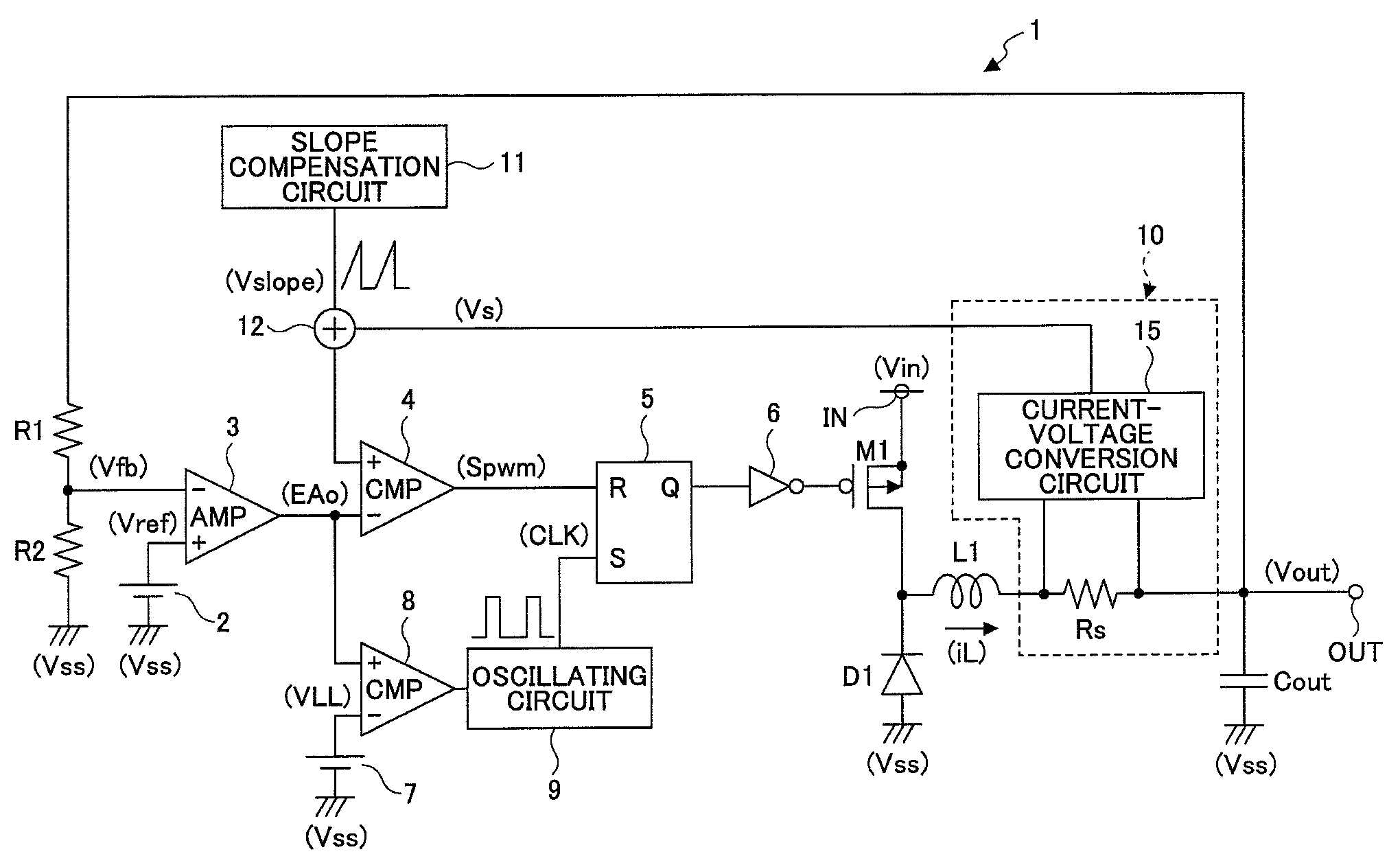
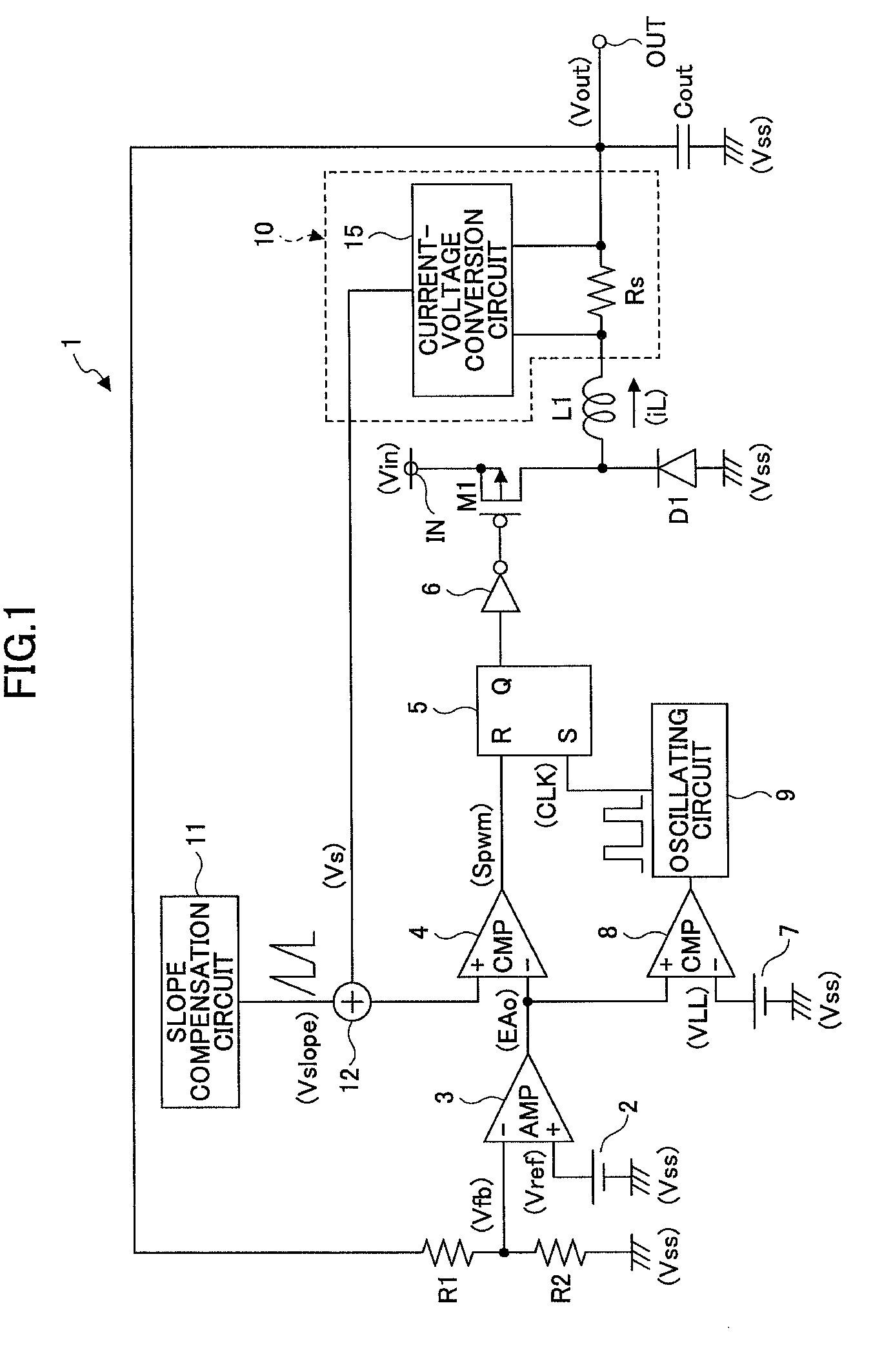
[0033]FIG. 1 illustrates a circuit example of a switching regulator according to a first embodiment of the present invention.

[0034]As shown in FIG. 1, a switching regulator 1 constitutes a step-down switching regulator employing an asynchronous rectification method, which steps down an input voltage Vin which has been input to an input terminal IN to a predetermined constant voltage, and outputs this voltage as an output voltage Vout from an output terminal OUT.

[0035]The switching regulator 1 includes a switching transistor M1 constituting a PMOS transistor, configured to perform a switching operation to implement output control of the input voltage Vin. The switching regulator 1 also includes a diode D1 constituting a flywheel diode for rectification.

[0036]The switching regulator 1 includes a reference voltage generating circuit 2 for generating a predetermined reference voltage Vref, resistors R1 and R2 for detecting the output voltage, an inductor L1, an output capacitor Cout, an...

second embodiment

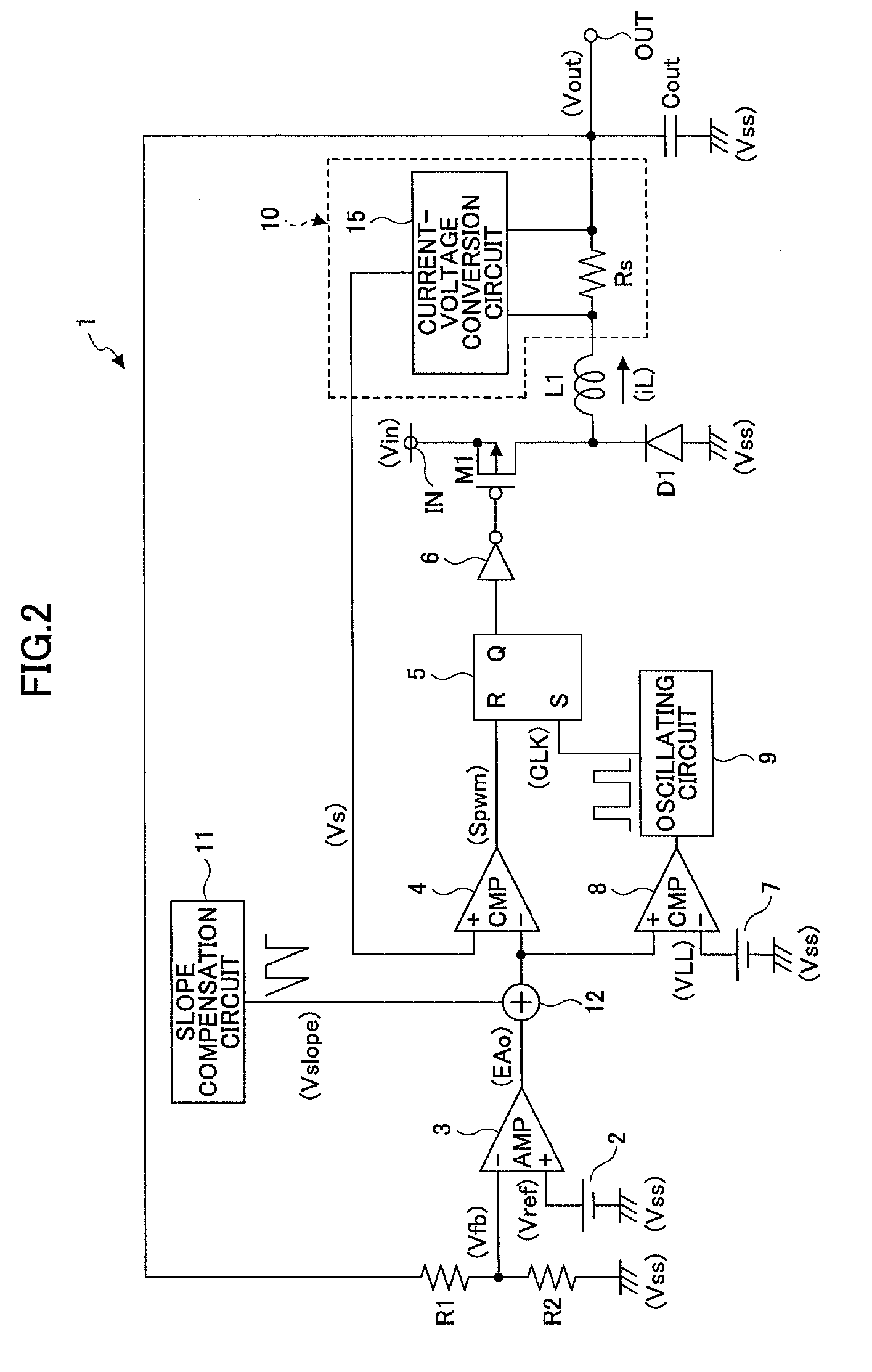
[0060]In the first embodiment, a switching regulator employing an asynchronous rectification method is taken as an example. The present invention is also applicable to a switching regulator employing a synchronous rectification method with which the power conversion efficiency can be improved. A second embodiment according to the present invention has such a configuration.

[0061]FIG. 4 illustrates a circuit example of a switching regulator according to the second embodiment of the present invention. In FIG. 4, elements corresponding to those in FIG. 1 are denoted by the same reference numbers, and are not further described. Only the different elements are described below.

[0062]The difference between FIG. 4 and FIG. 1 is that the circuit shown in FIG. 4 includes a synchronous rectification transistor M2 instead of the diode D1; a comparator 21 for detecting and preventing a reverse current, whereby the reverse current occurs when the inductor current iL flows from the output terminal ...


PUM


Abstract

In a switching regulator, a peak current value of an inductor current iL corresponding to a critical current is obtained by {(Vin−Vout) / Vin×Vout / L×Ts}, where Ts is the frequency of clock signals CLK constituting set pulses generated at predetermined timings by an oscillating circuit 9. Accordingly, by setting a reference voltage VLL as (Vout / L×Ts / rs), the peak current value of the inductor current iL when the load current has decreased is set to be the peak current value of the inductor current iL corresponding to the critical current. Therefore, simply by setting the reference voltage VLL in advance, the peak current of the inductor current iL when the load current has decreased is set to be the peak current value of the inductor current iL corresponding to the critical current.

Description

BACKGROUND OF THE INVENTION[0001]1. Field of the Invention[0002]The present invention relates to a technology of controlling a switching regulator constituting a DC-DC converter, and more particularly to a technology of controlling the switching regulator under light load conditions.[0003]2. Description of the Related Art[0004]The recent years have witnessed the increasing pervasiveness of compact mobile devices such as mobile phones. A compact secondary battery is used as the power source of such a compact mobile device. In order to reduce the size of the secondary battery and to maximize the usage time, attempts have been made to increase the performance of secondary batteries and to provide devices with higher energy saving capabilities.[0005]The efficiency of a switching regulator constituting a DC-DC converter is an important factor in increasing the energy saving capabilities of a device. Typically, this efficiency is expressed by a function of the output current flowing to th...

Claims


Application Information

Patent Timeline
IPC IPC(8): G05F1/10
CPCH02M2001/0025H02M3/156H02M1/0025
Inventor SHIMIZU, SHINYAMICHISHITA, YUUSUKE
Owner NISSHINBO MICRO DEVICES INC
Learn More