Display Device
a liquid crystal display and display device technology, applied in static indicating devices, non-linear optics, instruments, etc., can solve the problems of reducing the aperture ratio, and reducing the area occupied by the light shielding film in sub-pixels, so as to improve the aperture ratio of the display device
- Summary
- Abstract
- Description
- Claims
- Application Information
AI Technical Summary
Benefits of technology
Problems solved by technology
Method used
Image
Examples
first embodiment
[0050]In a first embodiment, an example in which the invention is applied to a fully transmissive liquid crystal display device of the IPS type will be described.
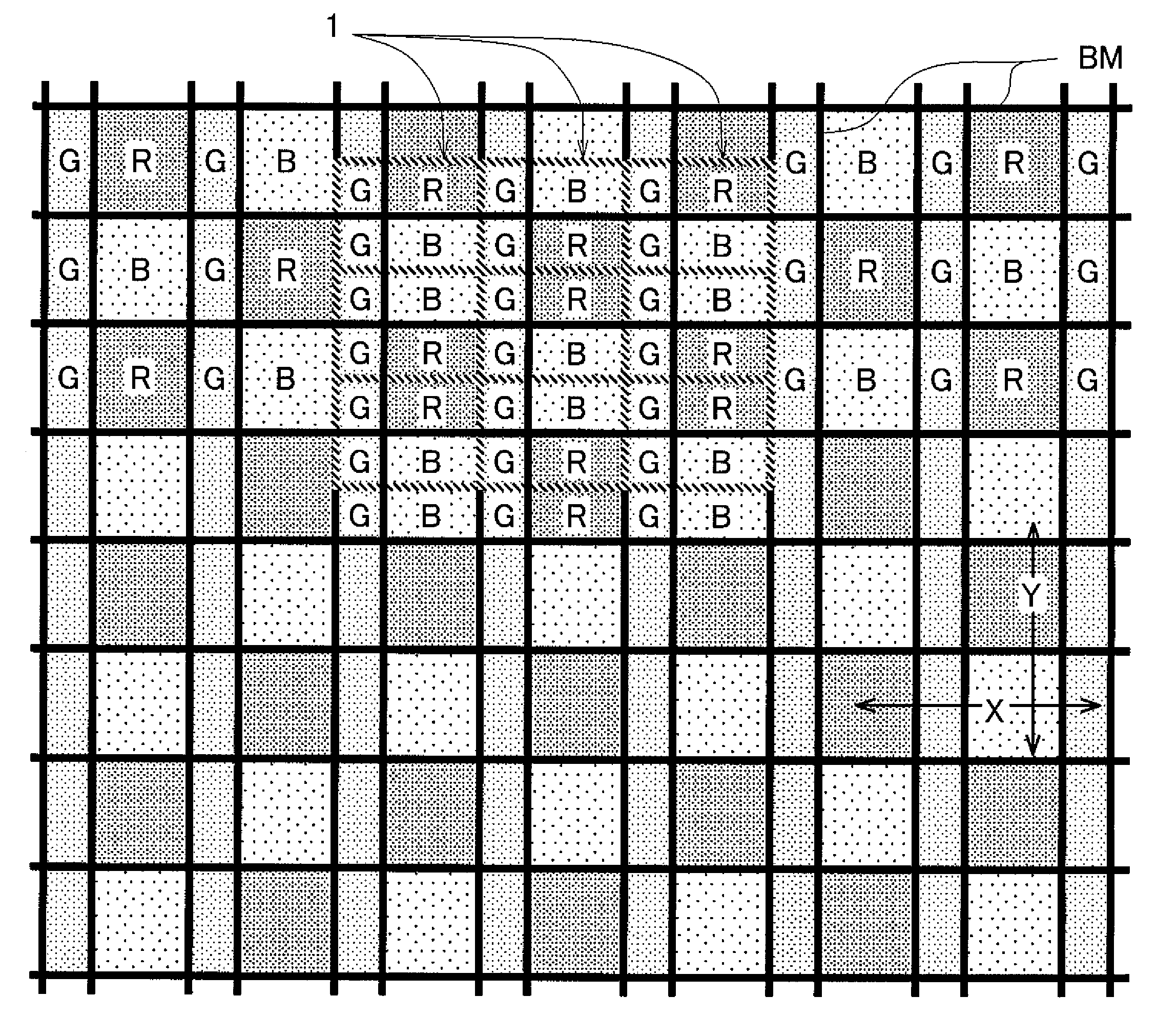
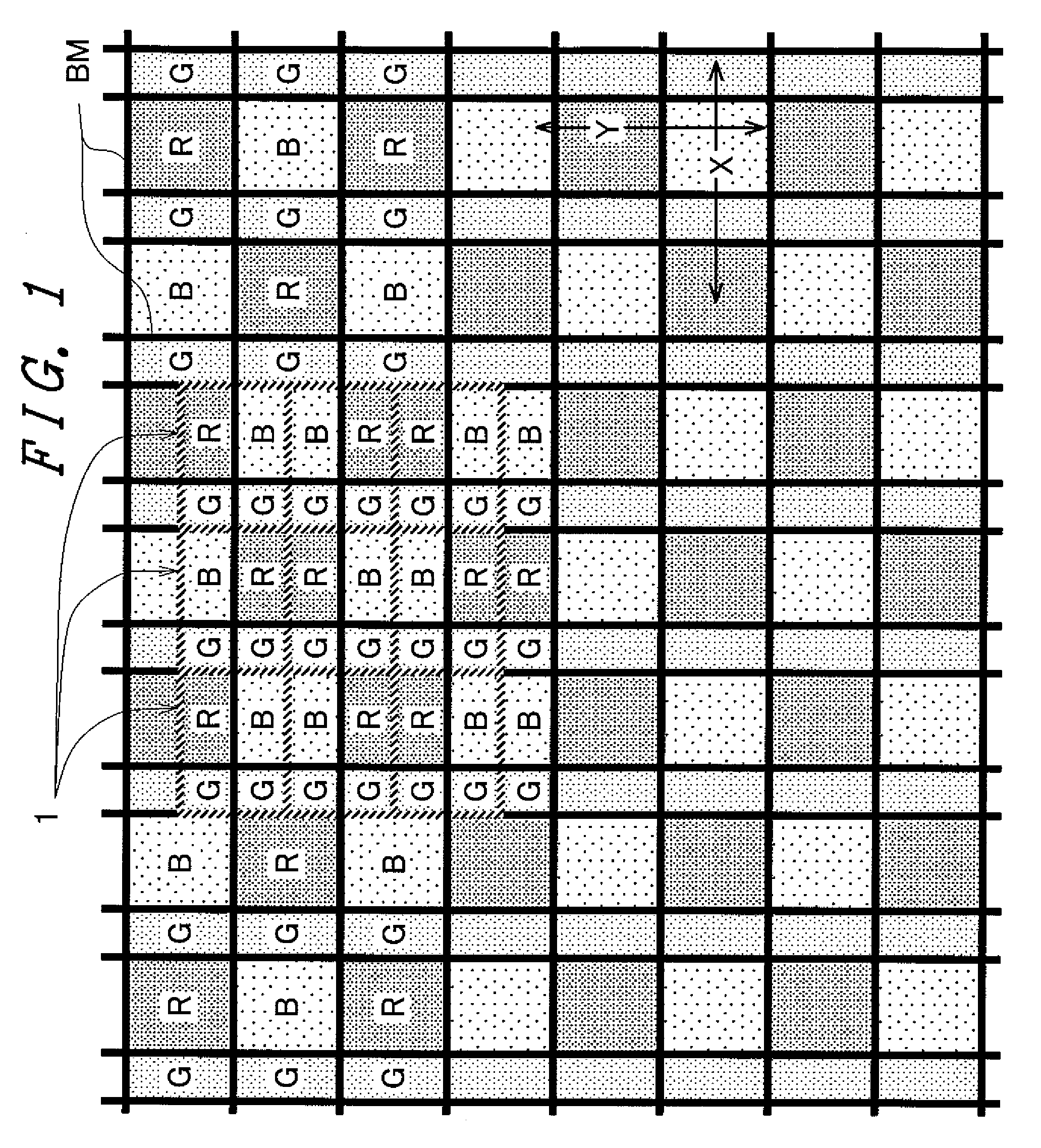
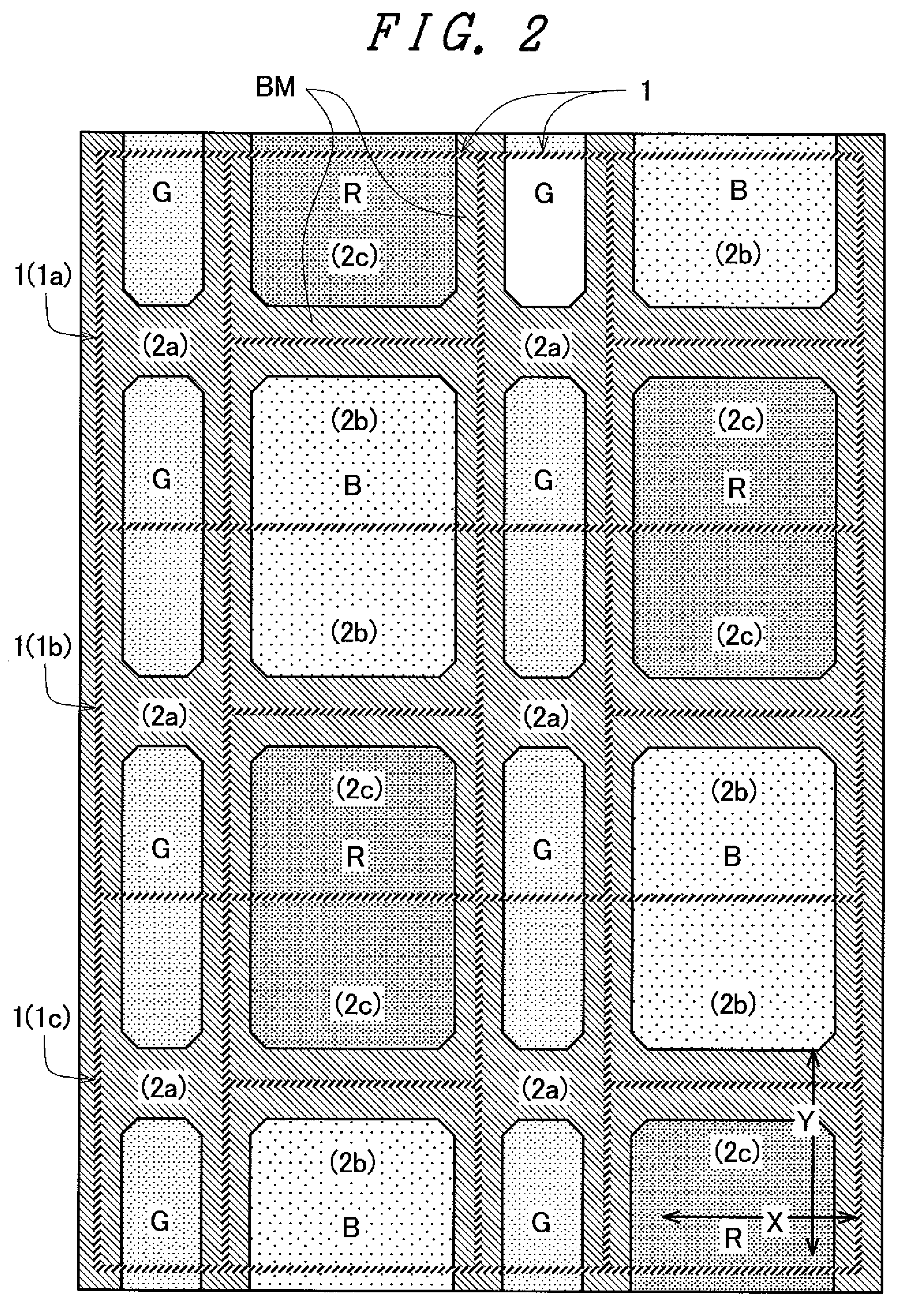
[0051]FIGS. 1 to 7 relate to the fully transmissive liquid crystal display device of the IPS type which is the first embodiment of the invention. FIG. 1 is a plan view showing an arrangement of color filters of a liquid crystal display panel. FIG. 2 is a partially enlarged plan view of FIG. 1. FIG. 3 is a plan view showing a configuration of pixels of FIG. 2 in a simplified manner. FIG. 4 is a plan view showing pixel electrodes and a counter electrode on a TFT substrate side of the liquid crystal display panel. FIG. 5 is a plan view showing the pixel electrodes, a scanning line, and video lines on the TFT substrate side of the liquid crystal display panel. FIG. 6 is a cross sectional view showing a cross sectional structure of the liquid crystal display panel taken along line A-A′ in FIG. 5. FIG. 7 is a cross sectional view...
second embodiment
[0086]FIG. 8 is a plan view showing an arrangement of color filters of a liquid crystal display panel in a fully transmissive liquid crystal display device of the IPS type of a second embodiment of the invention. FIG. 8 corresponds to FIG. 2 of the first embodiment.
[0087]The fully transmissive liquid crystal display device of the IPS type of the second embodiment has basically a similar configuration to that of the first embodiment but is different in the following point.
[0088]That is, as shown in FIG. 2, the light-shielding film BM between the second sub-pixel 2b and the third sub-pixel 2c is formed so as to cross the first sub-pixel 2a in the first embodiment. In the second embodiment, however, as shown in FIG. 8, the light-shielding film BM between the second sub-pixel 2b and the third sub-pixel 2c does not cross the first sub-pixel 2a but terminates in the second sub-pixel 2b and the third sub-pixel 2c.
[0089]In the thus configured second embodiment, the aperture ratio can be fu...
third embodiment
[0090]FIG. 9 is a plan view showing pixel electrodes, a scanning line, and video lines on a TFT substrate side of a liquid crystal display panel in a fully transmissive liquid crystal display device of the IPS type of a third embodiment of the invention.
[0091]The fully transmissive liquid crystal display device of the IPS type of the third embodiment has basically a similar configuration to that of the first embodiment but is different in the following point.
[0092]That is, a thin film transistor used as a switching element of each of the sub-pixels (2a, 2b, and 2c) is different. In the thin film transistor of the first embodiment, the pair of semiconductor regions functioning as a source region and a drain region are formed in the semiconductor layer 12 made of amorphous silicon. In the thin film transistor of the third embodiment, however, the pair of semiconductor regions functioning as a source region and a drain region are formed in a semiconductor layer PS made of polysilicon (...
PUM
 Abstract
Description
Claims
Application Information


