Supercharge Your Innovation With Domain-Expert AI Agents!

Current mirror circuit

Inactive Publication Date: 2009-12-24
SANYO SEMICON +1
View PDF1 Cites 1 Cited by
  • Summary
  • Abstract
  • Description
  • Claims
  • Application Information

AI Technical Summary

Benefits of technology

[0017]A current mirror circuit according to the present invention includes a first transistor wherein a base and a collector are short-circuited, and a second transistor wherein a base is connected to the base of the first transistor, and a current corresponding to a current flowing in the first transistor is permitted to flow in the second transistor. The circuit further comprises a compensation transistor wherein a gate is connected to the collector o

Problems solved by technology

In the current mirror circuits in FIGS. 1 and 2 constituted of bipolar transistors, errors caused by base current inevitably arise in principle.
Particularly, it is impossible to obtain sufficient accuracy when the hfe of the transistors is low or the mirror ratio is made larger.
However, when an emitter area ratio between transistors is changed and the mirror ratio is a value other than 1:1, the base current cannot be offset, and the mirror ratio changes.
However, because a current having 1 / hfe the collector current of the compensation transistor Q5 flows from Iin, this current.] often becomes a problem.
Although the current mirror circuits of FIGS. 3 and 4 constituted by MOS transistors do not employ a base current, the uniformity of the MOS transistors is inferior to that of a bipolar transistor.
Therefore, it is necessary to increase transistor size in order to achieve equal performance, which creates problems of frequency characteristic degradation, increased cost, or larger size caused by degradation in the degree of integration.
Furthermore, because the threshold voltage Vgs of the MOS transistor is larger than the threshold voltage Vbe of the bipolar transistor, a large dynamic range cannot be ensured, and it is difficult to apply MOS trangistors to a circuit having low power supply voltage.

Method used


Image

  • Current mirror circuit
  • Current mirror circuit
  • Current mirror circuit

Examples


Embodiment Construction

[0027]Hereinafter, embodiments of the present invention will be described based on the drawings.

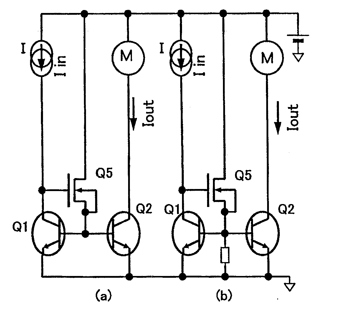
[0028]FIG. 5 shows a constitution of one embodiment. The current mirror circuit of FIG. 5(a) has a constitution corresponding to (d) in FIGS. 1 to 4.

[0029]The collector of a bipolar NPN-type transistor Q1 is connected to a positive power supply via a current generator I, and the emitter is connected to ground. Further, the collector of a bipolar NPN-type transistor Q2 is connected to the positive power supply via a load M, and the emitter is connected to ground. Further, the bases of the transistors (Q1,Q2) are directly connected to each other. Then, the circuit has an N-channel MOS-type compensation transistor Q5, in which the gate of the compensation transistor Q5 is connected to the collector of the transistor Q1, the drain is connected to the positive power supply, and the source is connected to the bases of the transistors (Q1,Q2).

[0030]Thus, the base current of the transistors (Q1,Q...


PUM


Abstract

A current mirror circuit includes a first transistor, a plurality of second transistors whose bases are connected to a base of the first transistor, and a compensation transistor having a gate connected to a collector of the first transistor, a source and a back gate connected to the base of the first transistor and the bases of the plurality of second transistors, and a drain connected to a power source. The first transistor and the plurality of second transistors are bipolar transistors. The compensation transistor is a MOS-type transistor. A current corresponding to a current flowing in the first transistor is permitted to flow in the plurality of second transistors.

Description

TECHNICAL FIELD[0001]The present invention relates to a current mirror circuit that includes a first transistor wherein a base and a collector are short-circuited and a second transistor wherein a base is connected to the base of the first transistor, and wherein a current corresponding to a current flowing in the first transistor is made to flow in the second transistor.BACKGROUND ART[0002]Conventionally, a large number of current mirror circuits have been used in semiconductor integrated circuits, among known current mirror circuits are those illustrated in FIG. 1, FIG. 2, FIG. 3, and FIG. 4.[0003]FIG. 1 shows a circuit using NPN-transistors, and FIG. 1(a) shows a constitution of a basic current mirror circuit.[0004]The collector of the transistor Q1 is connected to a positive power supply via a current generator I, and the emitter is connected to the ground. Further, the collector of the transistor Q2 is connected to a positive power supply via a load M, and the emitter is connec...

Claims


Application Information

Patent Timeline
IPC IPC(8): G05F3/02
CPCH03F3/343G05F3/267
Inventor HASHIMOTO, FUMINORI
Owner SANYO SEMICON
Features
  • R&D
  • Intellectual Property
  • Life Sciences
  • Materials
  • Tech Scout
  • Unparalleled Data Quality
  • Higher Quality Content
  • 60% Fewer Hallucinations
Learn More