Multilayer ceramic electronic component and manufacturing method thereof

Active Publication Date: 2009-12-24
MURATA MFG CO LTD
View PDF29 Cites 26 Cited by
  • Summary
  • Abstract
  • Description
  • Claims
  • Application Information

AI Technical Summary

Benefits of technology

[0026]Therefore, when forming a primary plated film of the external terminal electrode by direct plating such that the primary plated film covers the exposed end distribution area, an edge of the primary plated film is straight or substantially s

Problems solved by technology

This degrades the characteristics.
If a typical method of printing a thick film paste is used, there is a limit to the accuracy of the paste application.
Therefore, it is difficult to form external terminal electrodes with high accuracy.
This phenomenon is problematic particularly when forming external terminal electrodes by direct plating.
If the e

Method used


Image

  • Multilayer ceramic electronic component and manufacturing method thereof
  • Multilayer ceramic electronic component and manufacturing method thereof
  • Multilayer ceramic electronic component and manufacturing method thereof

Examples


Example

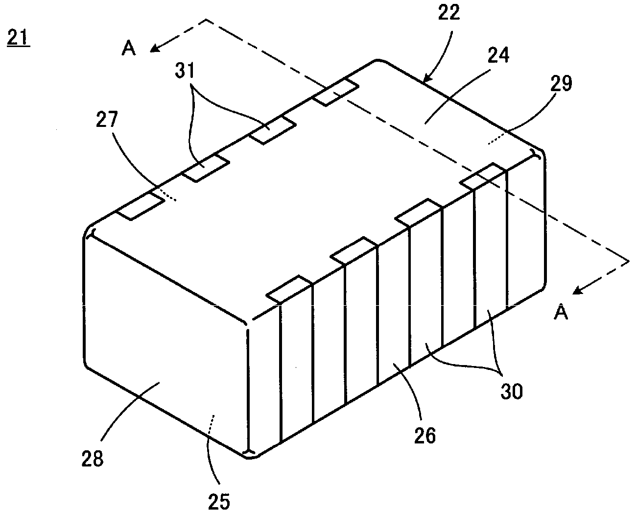
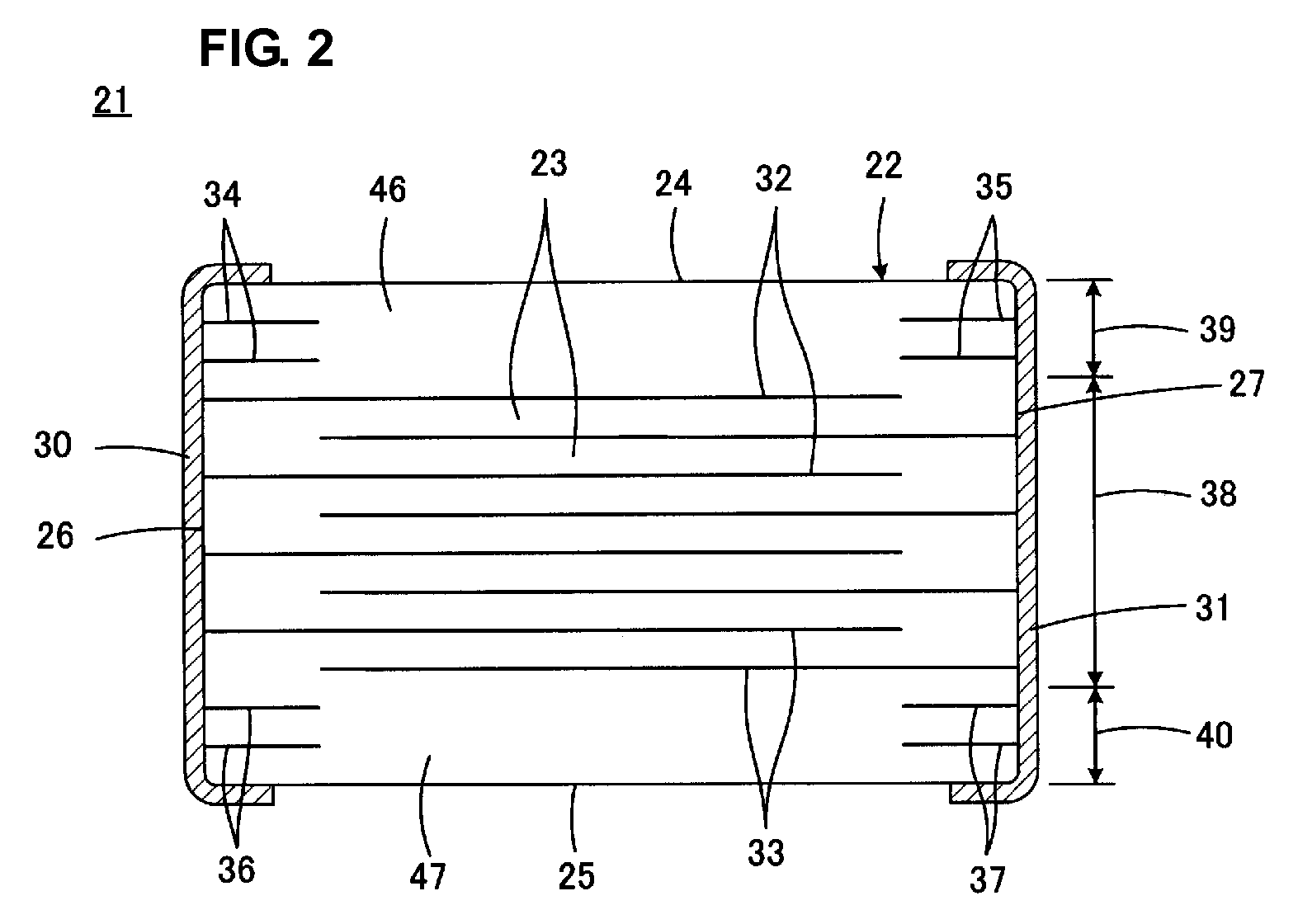
[0044]FIGS. 1 to 6 are drawings showing a multilayer ceramic electronic component 21 according to a first preferred embodiment of the present invention. FIG. 1 is a perspective view showing the multilayer ceramic electronic component 21. FIG. 2 is a sectional view taken along line A-A of FIG. 1. FIGS. 3A to 3F are plan views showing an internal structure of a ceramic element 22 included in the multilayer ceramic electronic component 21 shown in FIG. 1.

[0045]As shown in FIGS. 1 to 3, the ceramic element 22 included in the multilayer ceramic electronic component 21 is formed by laminating a plurality of ceramic layers 23. The ceramic element 22 has a first main surface 24 and a second main surface 25, which are opposed to each other, and a first side surface 26, a second side surface 27, a third side surface 28, and a fourth side surface 29 connecting the main surfaces 24 and 25. The first side surface 26 and second side surface 27 are opposed to each other, and the third side surface...


PUM

PropertyMeasurementUnit
Thicknessaaaaaaaaaa
Widthaaaaaaaaaa
Areaaaaaaaaaaa

Abstract

A multilayer ceramic electronic component includes dummy conductor patterns on a ceramic green sheet laminated in an earlier stage of the lamination and sheet-by-sheet crimping process that have widths that are less than the widths of dummy conductor patterns on a ceramic green sheet laminated in a later stage of the lamination and sheet-by-sheet crimping process.

Description

BACKGROUND OF THE INVENTION[0001]1. Field of the Invention[0002]The present invention relates to a multilayer ceramic electronic component and a manufacturing method thereof. In particular, the present invention relates to a multilayer ceramic electronic component in which an external terminal electrode is coupled not only to an exposed end of an internal electrode but also to an exposed end of a dummy conductor so as to improve the fixing strength of the external terminal electrode, and a method for manufacturing such a multilayer ceramic electronic component.[0003]2. Description of the Related Art[0004]In recent years, electronic apparatuses, such as cell phones, notebook personal computers, digital still cameras, and digital audio systems have been downsized. These electronic apparatuses use many downsized, high-performance, multilayer ceramic electronic components.[0005]Generally, a multilayer ceramic electronic component includes a ceramic element including a plurality of ceram...

Claims


Application Information

Patent Timeline
IPC IPC(8): H01G4/228B32B37/00
CPCH01G4/012H01G4/30H01G4/232
Inventor TANIGUCHI, TAKUMIMATSUMOTO, HIROYUKI
Owner MURATA MFG CO LTD
Why Eureka
Try Eureka