Solid-state imaging device

Inactive Publication Date: 2009-12-31
PANASONIC CORP
View PDF8 Cites 43 Cited by
  • Summary
  • Abstract
  • Description
  • Claims
  • Application Information

AI Technical Summary

Benefits of technology

[0017]This structure allows removing the difference in signal levels of the Gr pixels and the Gb pixels on which the green color filters are arranged, which make up half of the pixels in the Bayer pattern, caused by the crosstalk due to the difference in the signal levels of the Gr pixels and the Gb pixels and the signal levels of the R pixels and the B pixels. Therefore, it is possi

Problems solved by technology

This causes a problem that a unifor

Method used


Image

  • Solid-state imaging device
  • Solid-state imaging device
  • Solid-state imaging device

Examples


embodiment 1

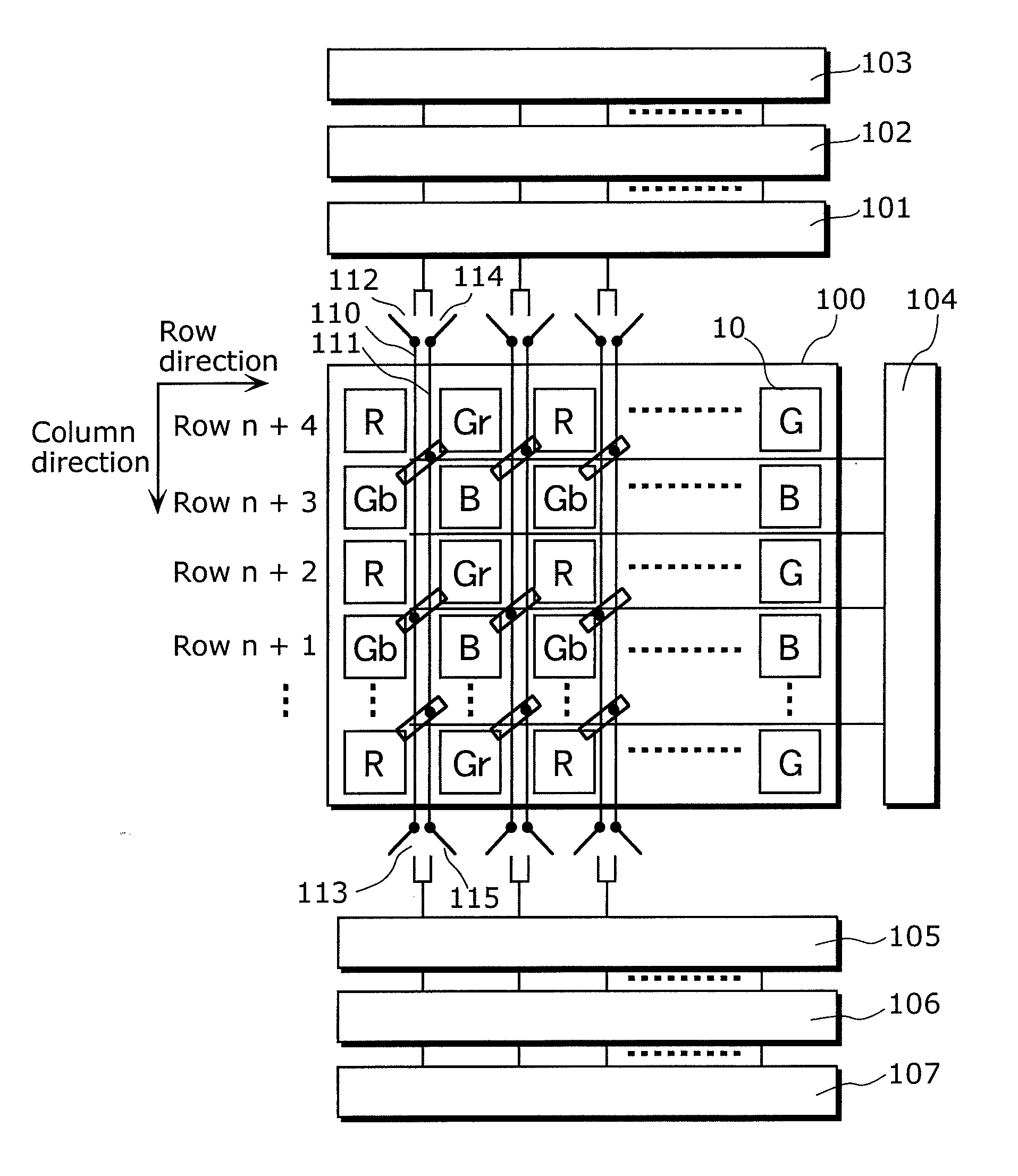
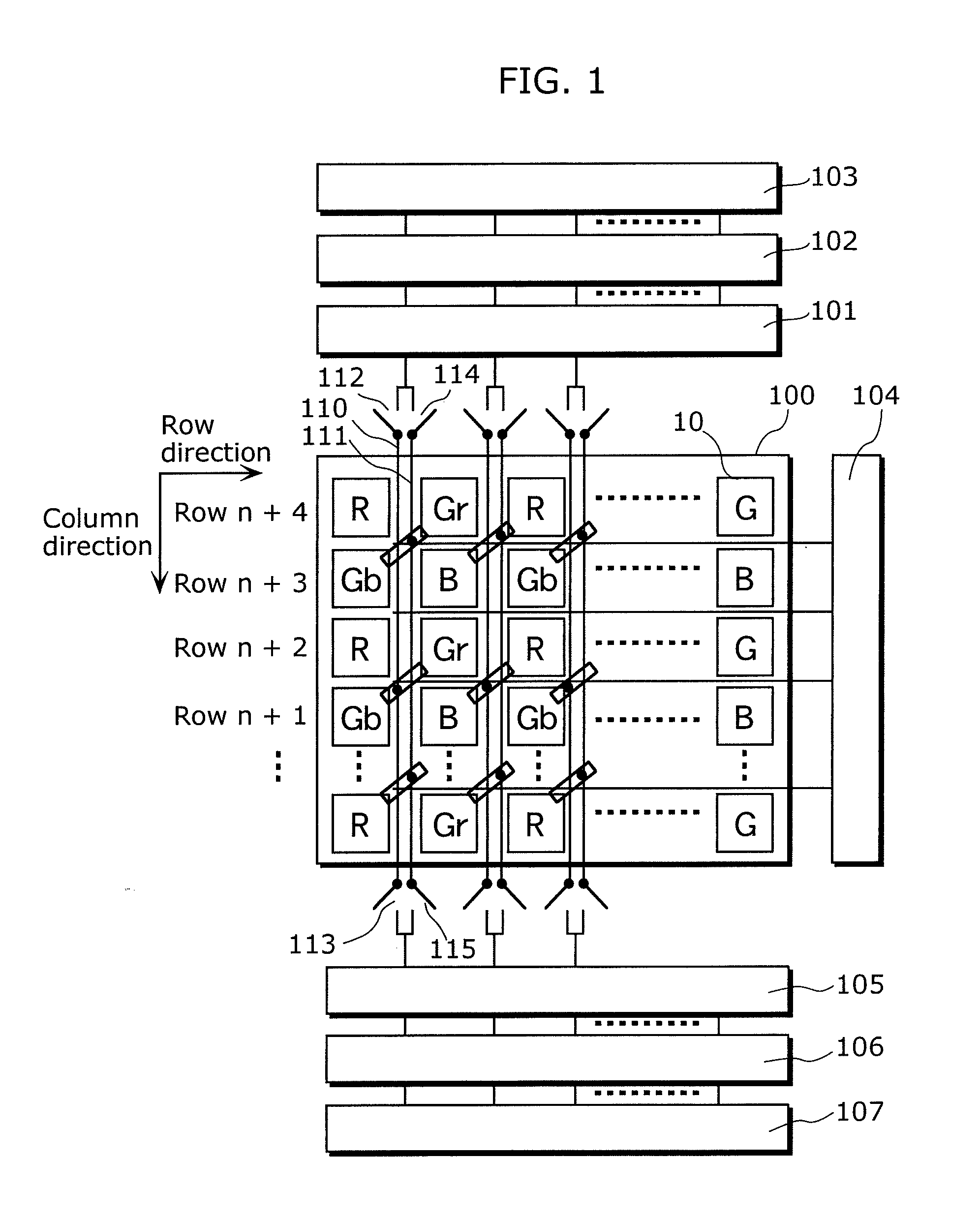
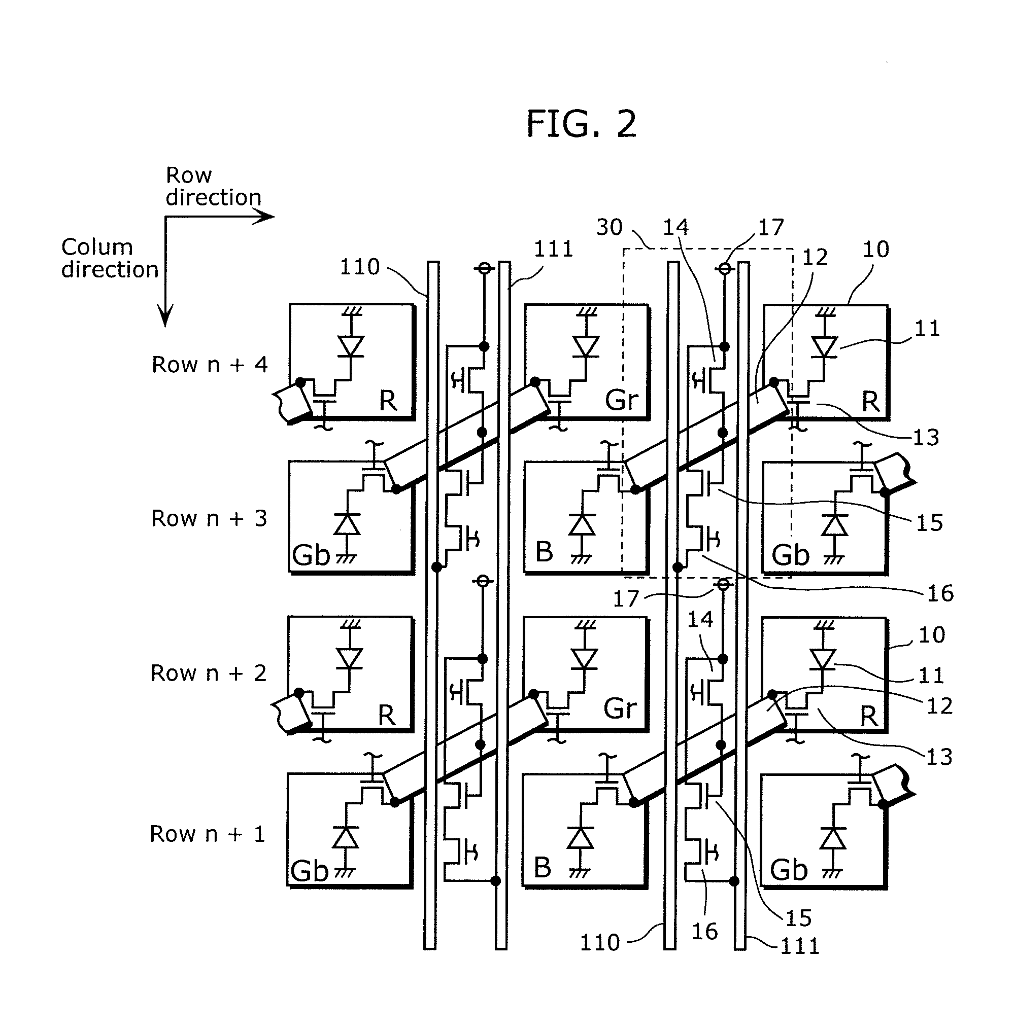
[0027]FIG. 1 illustrates the structure of the solid-state imaging device according to Embodiment 1 of the present invention, and FIG. 2 illustrates the structure of pixel cells 10 configuring a pixel area 100 of the solid-state imaging device.

[0028]The solid-state imaging device includes, as shown in FIG. 1, the pixel area 100 in which plural pixel cells 10 are arranged in a matrix form (in rows and columns), column circuits 101 and 105, AD converters 102 and 106, row scanning circuits 103 and 107, respectively provided above and below the pixel area 100 for each column of the pixel cell 10, a column scanning circuit 104, column signal lines 110 and 111 (the first column signal line 110 and the second column signal line 111), and switches 112, 113, 114, and 115.

[0029]Each of the pixel cells 10 outputs signals according to the intensity of incident light. Color filters having two or more colors are respectively arranged on the light incidence plane of the pixel cells 10. More specifi...

embodiment 2

[0057]FIG. 3 illustrates the structure of the solid-state imaging device according to Embodiment 2 of the present invention. Furthermore, FIG. 4 illustrates the structure of pixel cells 20 in the solid-state imaging device. Note that the structure other than the structure illustrated in FIGS. 3 and 4 which shall be described later is identical to the solid-state imaging device according to Embodiment 1 of the present invention.

[0058]The solid-state imaging device includes, as shown in FIG. 3, the pixel area 200 in which plural pixel cells 20 are arranged in a matrix form, column circuits 201 and 205, AD converters 202 and 206, row scanning circuits 203 and 207, respectively provided above and below the pixel area 200 for each column of the pixel cells 20, a column scanning circuit 204, column signal lines 210 and 211 (the first column signal line 210 and the second column signal line 211), and switches 212, 213, 214, and 215.

[0059]Each of the pixel cells 20 outputs signals according...


PUM


Abstract

It is an object of the present invention to provide a solid-state imaging device capable of operating at high-speed, and suppressing the deterioration of image quality caused by coupling. A solid-state imaging device according to the present invention includes: pixels arranged in rows and columns; color filters each of which is arranged on a light incidence plane of a corresponding one of the pixels, each of the color filters being one of at least two colors; and column signal lines provided for each of the columns of the pixels, and each of which transmits the signals from the pixels in a column direction, in which one of the color filters is arranged on one of the pixels connected to the column signal line, and is of a same color as another one of the color filters arranged on another one of the pixels connected to the column signal line.

Description

BACKGROUND OF THE INVENTION[0001](1) Field of the Invention[0002]The present invention relates to an amplifying (MOS) solid-state imaging device which amplifies and takes out signal charge generated in a photoelectric conversion unit, and particularly relates to a solid-state imaging device equipped with color filters.[0003](2) Description of the Related Art[0004]In recent years, CCD and MOS solid-state imaging devices used for video cameras and electronic still cameras have significantly developed to a point where the size of a unit pixel is miniaturized to 2 μm2 or less and the number of pixels exceeds 10 million pixels. Furthermore, there is an increasing request for accelerating the read-out time which is a tradeoff with the increase in the number of pixels. Thus, it is necessary to maintain the frame rate despite the increase in the number of pixels. Accordingly, even if the number of pixels increases, it is necessary for the solid-state imaging devices to secure higher image q...

Claims


Application Information

Patent Timeline
IPC IPC(8): H04N5/335H01L27/14H01L27/146H04N9/07
CPCH01L27/14603H01L27/14621H01L27/14641H04N5/37457H04N5/378H04N5/335H04N25/00H04N25/778H04N25/75
Inventor KYOGOKU, MASANORISHIMOMURA, KENICHI
Owner PANASONIC CORP
Why Eureka
Try Eureka