
Substrate for a display panel, a display panel having the substrate, a production process of the substrate, and a production process of the display panel

Active Publication Date: 2010-01-07
SHARP KK
View PDF3 Cites 16 Cited by
  • Summary
  • Abstract
  • Description
  • Claims
  • Application Information

AI Technical Summary

Benefits of technology

[0012]In order to overcome the problems described above, preferred embodiments of the present invention provide a substrate for a display panel by which insulation breakdown of an insulating film can be prevented, a display panel having the substrate, a production process of the substrate and a production process of the display panel, and a substrate for a display panel by which insulation breakdown of an insulating film which occurs in a production process due to electrical discharge between two conductive films between which an insulating film is sandwiched can be prevented, a display panel having the substrate, a production process of the substrate and a production process of the display panel.
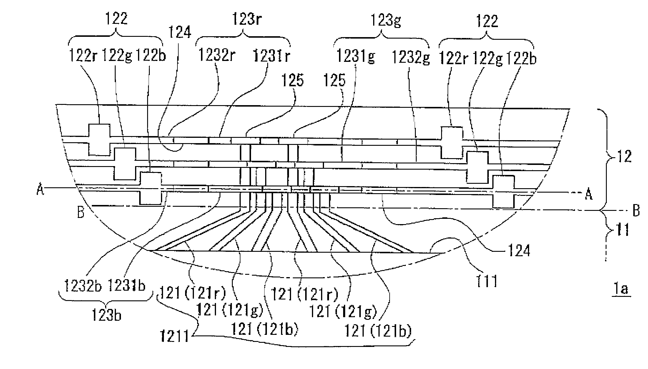
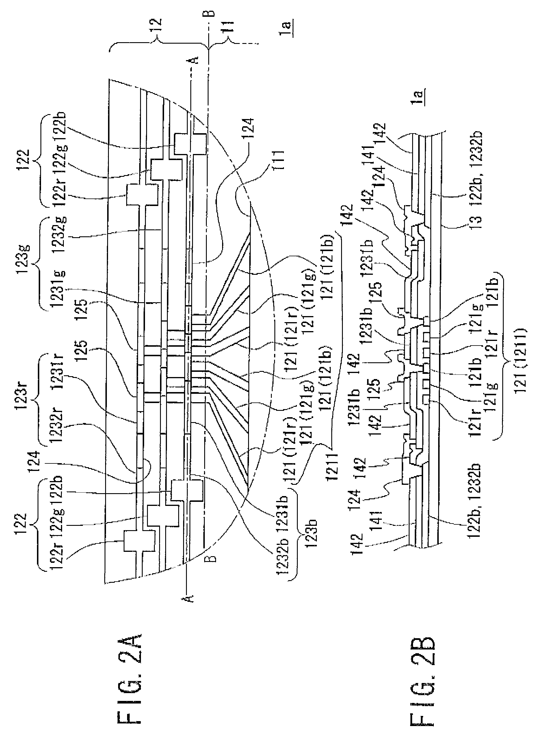
[0027]According to the preferred embodiments of the present invention, a difference between an area of the line drawn from the bus line in the display region and an area of the portion of the inspection line which overlaps with the line drawn from the bus line between which the insulating film is sandwiched can be reduced. Accordingly, a potential difference can be narrowed between the line drawn from the bus line in the display region and the portion overlapping with the line drawn from the bus line between which the insulating film is sandwiched, and electrical discharge between them is prevented or suppressed, and therefore insulation breakdown of the insulating film provided between them can be prevented or suppressed.
[0028]Especially when the relation between the area of the line drawn from the bus line and the area of the inspection line satisfies the above-mentioned formula, electrical discharge between the line drawn from the bus line and the inspection line is prevented more reliably, and therefore insulation breakdown of the insulating film can be prevented.
[0029]In addition, according to the preferred embodiments of the present invention, it is not necessary to additionally include steps of forming the inspection line and other elements, which creates no increase in the production cost.

Problems solved by technology

In the TFT array substrate having the above-described configuration, when the insulating film between the conductive films is broken and the conductive films are electrically connected at a position different from a designed position in a different manner, the TFTs, the data signal lines, the gate signal lines and other elements do not function sometimes as designed, which could cause display defects in the display panel.
In addition, when the insulating film is broken in the inspection line bundles, the lighting inspection of the display panel cannot be performed successfully.
As a result thereof, the presence of display defects in the display panel and their appearance cannot be detected accurately, and a problem therefore arises in quality control.
Causes of the break in the insulating film include electrical discharge resulting from a potential difference between the conductive films between which the insulating film is sandwiched.
After static electricity is built up in the conductive films, when the potential difference between the conductive films between which the insulating film is sandwiched goes beyond a withstand voltage of the insulating film, electrical discharge is made between the conductive films, and therefore insulation breakdown of the insulating film occurs.
However, in the TFT array substrate having the above-described configuration, it is necessary that portions where source bus lines and gate bus lines are interconnected are placed on the substrate, so that design limitation is imposed on the substrate.

Method used


Image

  • Substrate for a display panel, a display panel having the substrate, a production process of the substrate, and a production process of the display panel
  • Substrate for a display panel, a display panel having the substrate, a production process of the substrate, and a production process of the display panel
  • Substrate for a display panel, a display panel having the substrate, a production process of the substrate, and a production process of the display panel

Examples


Embodiment Construction

[0043]A detailed description of a substrate for a display panel according to preferred embodiments of the present invention will now be given with reference to the accompanying drawings.

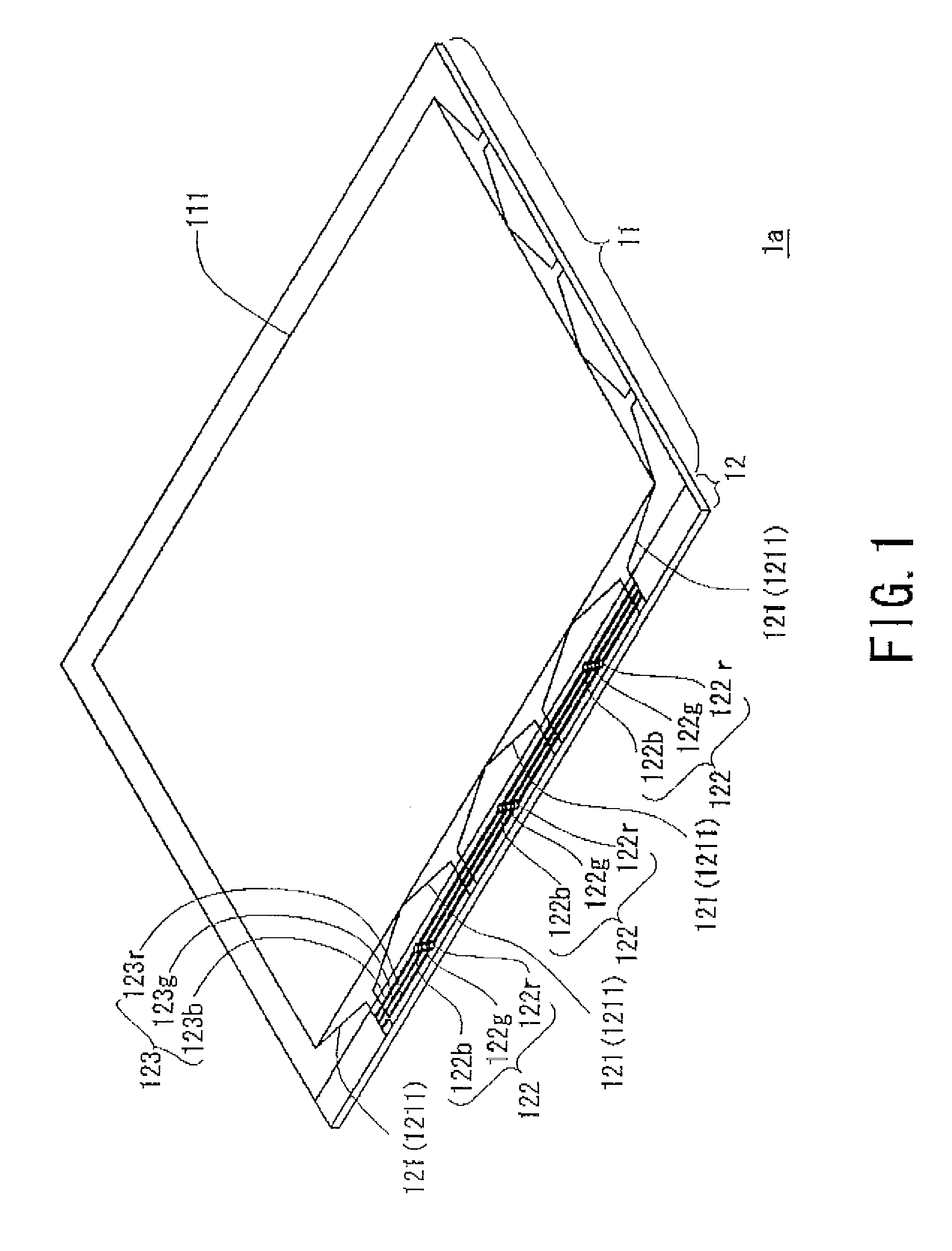
[0044]FIG. 1 is an external perspective view schematically showing a configuration of a substrate for a display panel according to a first preferred embodiment of the present invention. Firstly, an entire configuration of a substrate 1a for a display panel according to the first preferred embodiment of the present invention will be described.

[0045]As shown in FIG. 1, the substrate 1a for a display panel according to the first preferred embodiment of the present invention includes a section 11 where a display region 111 is provided (hereinafter, referred to as the “main body section 11”), and a section 12 where lines for lighting inspection of a display panel and other elements are provided (hereinafter, referred to as the “inspection line section 12”.

[0046]In the display region 111 of the main body s...


PUM


Abstract

A substrate for a display panel in which insulation breakdown of an insulating film can be prevented, a display panel having the substrate, a production process of the substrate and a production process of the display panel.The substrate includes an inspection line 123 for transferring a signal for inspection which includes a first section 1231 including a portion overlapping with and / or intersecting an input line 121 drawn from a data signal line in a display region 111 between which an insulating film 141 is sandwiched and a second section 1232 which includes a portion other than the portion overlapping with and / or intersecting the input line 121 which are formed to be electrically independent from each other and are arranged to be electrically connected by a conductor 128, wherein a difference between areas of the first section 1231 and the input line 121 is reduced.

Description

BACKGROUND OF THE INVENTION[0001]1. Field of the Invention[0002]The present invention relates to a substrate for a display panel, a display panel having the substrate, a production process of the substrate and a production process of the display panel, and specifically relates to a substrate for a display panel such as a substrate for a liquid crystal panel having a layered structure which includes conductive films, semiconductive films and insulating films with given patterns, a display panel having the substrate, a production process of the substrate and a production process of the display panel.[0003]2. Description of the Related Art[0004]Some liquid crystal display panels include a TFT array substrate and a color filter which are disposed opposed to each other leaving a tiny space therebetween, and the space is filled with a liquid crystal.[0005]On one surface of the TFT array substrate, thin films including conductive films, semiconductive films and insulating films with given ...

Claims


Application Information

Patent Timeline
IPC IPC(8): H05K1/00H05K3/00
CPCG02F1/1309G02F1/1345Y10T29/49155H01L27/3276G02F2001/136254G02F1/136254H10K59/131
Inventor HIRAKATA, YOSHIOTSUBATA, TOSHIHIDEMATSUDA, MASAHIRO
Owner SHARP KK
Learn More