Supercharge Your Innovation With Domain-Expert AI Agents!

Probe apparatus, a process of forming a probe head, and a process of forming an electronic device

a technology of probe head and probe body, which is applied in the direction of contact member manufacturing, semiconductor/solid-state device testing/measurement, instruments, etc., can solve the problems of wear of the test probe conductor

Active Publication Date: 2010-01-21
MONTEREY RES LLC
View PDF17 Cites 7 Cited by
  • Summary
  • Abstract
  • Description
  • Claims
  • Application Information

AI Technical Summary

Problems solved by technology

Moving the test probes is time-consuming and results in wear of the test probe conductors.

Method used


Image

  • Probe apparatus, a process of forming a probe head, and a process of forming an electronic device
  • Probe apparatus, a process of forming a probe head, and a process of forming an electronic device
  • Probe apparatus, a process of forming a probe head, and a process of forming an electronic device

Examples


Embodiment Construction

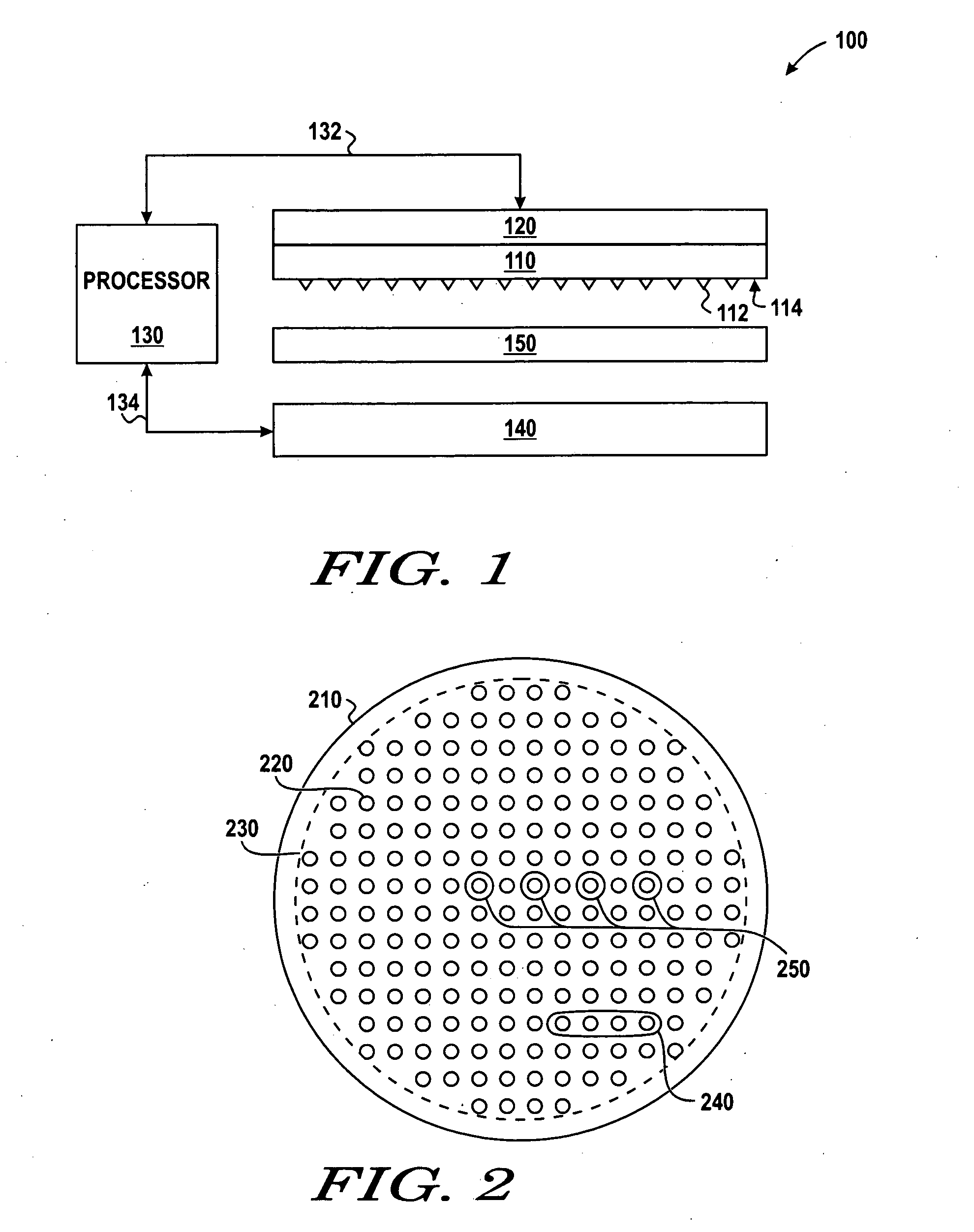
[0028]A workpiece, such as an electronic device workpiece, can include conductive and non-conductive materials. At various points of time during a manufacturing process, or during the development of the manufacturing process, analysis of electrical properties of these materials can be performed using test probes. Test probes can be part of a probe head and can include conductors used to provide electrical contact with the workpiece and to conduct signals between the workpiece and test equipment, such as electronic instrumentation. A probe apparatus and process disclosed herein includes a set of conductors. These conductors can span a significant portion or substantially all of a surface of the workpiece. A subset of the conductors can be activated while another subset can be or remain deactivated. Thus, different probe geometries can be realized, and different probing events can be accomplished without separating and subsequent contacting of the conductors and the workpiece.

[0029]In...


PUM

PropertyMeasurementUnit
areaaaaaaaaaaa
areaaaaaaaaaaa
diameteraaaaaaaaaa

Abstract

A probing apparatus includes a set of conductors configured to contact a surface of a workpiece simultaneously. A processor activates subsets of the conductors to determine a four-point-probe parameter, wherein the subset is less than the set of conductors. Another subset determines another four-point-probe parameter. The set of conductors remain in contact with the surface of the workpiece during and between activating each subset. A process of forming a probe head includes a probe substrate and associated conductive leads. An insulating layer is formed over the probe substrate and patterned to expose the leads. Conductors, connected to the leads, are formed over the insulating layer and define a probing area of at least 250 cm2. A process of forming an electronic device includes contacting a surface of a workpiece using conductors. Subsets of the conductors are activated to determine four-point-probe parameters at different areas of the workpiece.

Description

BACKGROUND[0001]1. Field of the Disclosure[0002]This disclosure relates to a probe apparatus, a process of forming a probe head, and a process of forming an electronic device.[0003]2. Description of the Related Art[0004]Test probes are extensively used during the development of an integrated circuit (IC) fabrication process as well as during the manufacturing process of the IC components. One type of test probe, the four-point probe, is used to measure the electrical resistance of metal and semiconductor materials. Electrical resistance measurements often are performed at multiple sites on a workpiece. Testing is typically performed in a serial manner wherein the test probes, and four-point probes, in particular, are relocated to subsequent sites after completing measurements at a previous site. Moving the test probes is time-consuming and results in wear of the test probe conductors.BRIEF DESCRIPTION OF THE DRAWINGS[0005]The present disclosure may be better understood, and its nume...

Claims


Application Information

Patent Timeline
Patent Type & Authority Applications(United States)
IPC IPC(8): G01R1/073H01R43/00
CPCG01R1/07385G01R3/00G01R31/2831Y10T29/49204H01L21/76877H01L22/14H01L29/7833H01L21/7684
Inventor WEDLAKE, MICHAEL D.
Owner MONTEREY RES LLC
Features
  • R&D
  • Intellectual Property
  • Life Sciences
  • Materials
  • Tech Scout
  • Unparalleled Data Quality
  • Higher Quality Content
  • 60% Fewer Hallucinations
Learn More