

Gate Driving Circuit
- Summary
- Abstract
- Description
- Claims
- Application Information
AI Technical Summary
Benefits of technology
Problems solved by technology
Method used
Image

Examples
Embodiment Construction
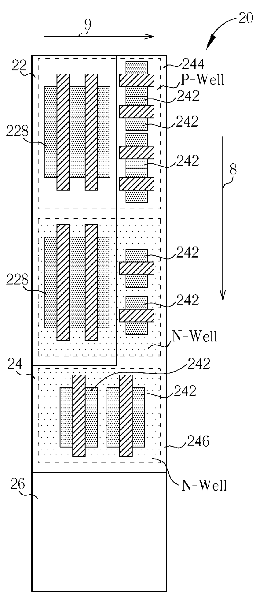
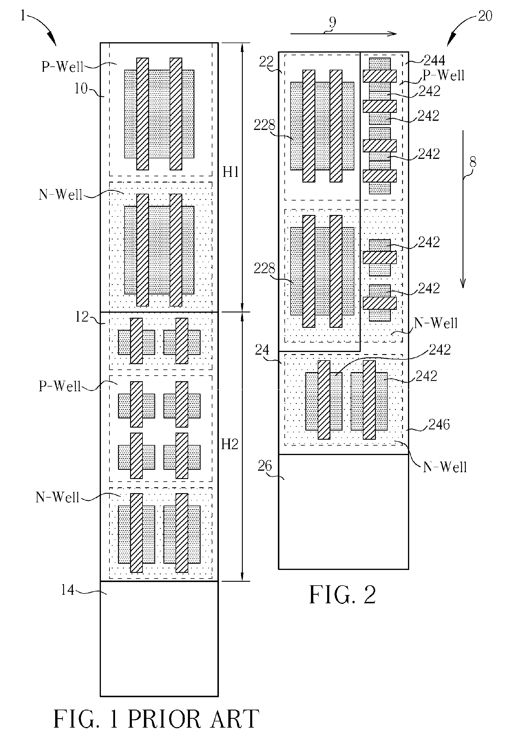
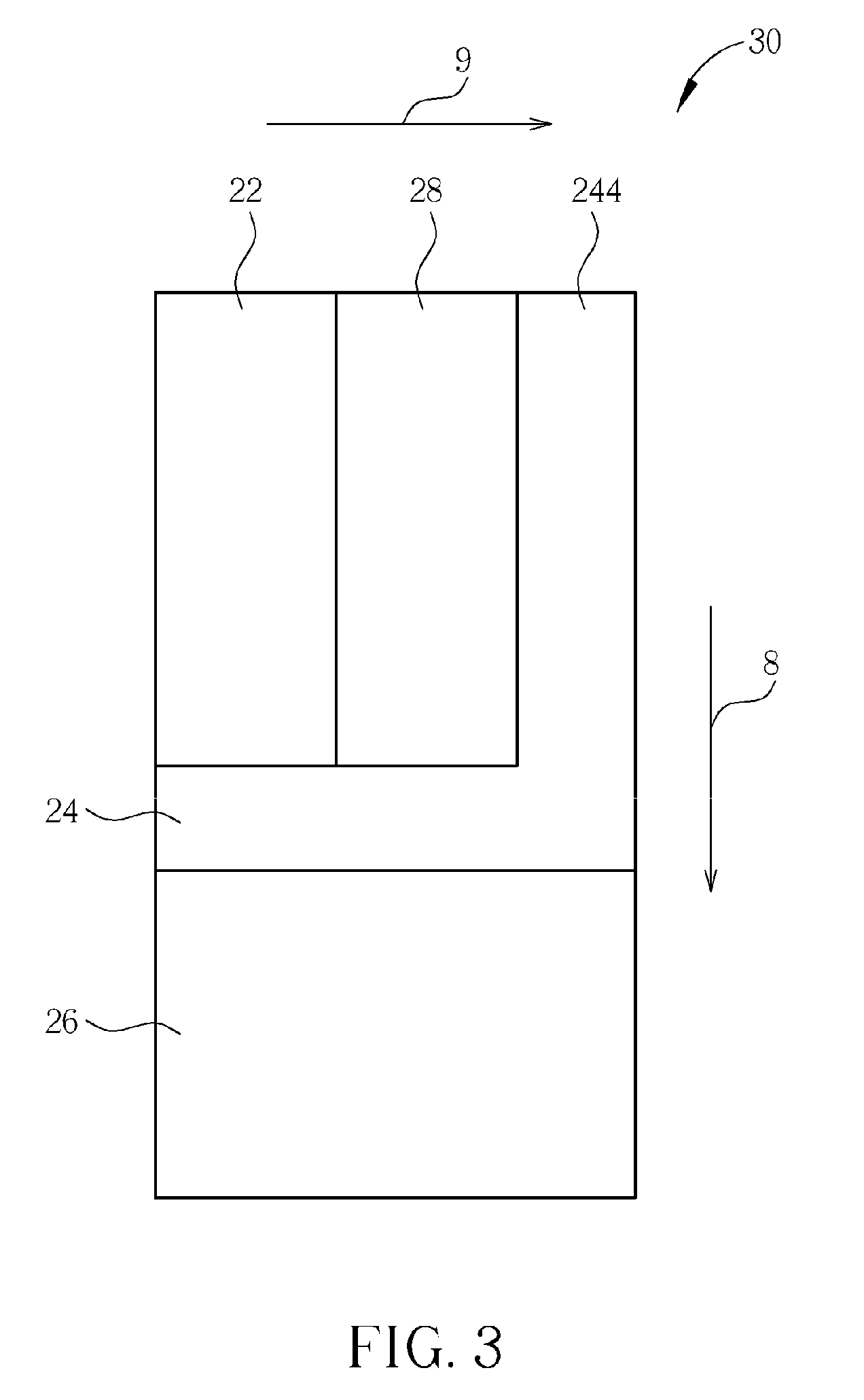
[0018]Please refer to FIG. 2, which is a schematic diagram of a single channel layout 20 of a gate driving circuit according to an embodiment of the present invention. The gate driving circuit is utilized for driving thin film transistors of a LCD, and is implemented with an integrated circuit. The gate driving circuit comprises a first output buffer unit region 22, a level shifter region 24 and a low voltage circuit region 26.
[0019]The first output buffer unit region 22 is formed on a plane, which is not shown in FIG. 2, and is utilized for setting a first output buffer unit 228. The level shifter region 24 is formed on the plane for setting a level shifter 242, and includes a vertical region 244 and a horizontal region 246 connected to the vertical region 244. The vertical region 244 and the first output buffer unit region 22 are aligned in a horizontal direction of the plane, which is the direction indicated by the arrow 9. The horizontal region 246 is located beneath the vertica...
PUM
 Abstract
Description
Claims
Application Information