Electronic packaging structure and a manufacturing method thereof

Inactive Publication Date: 2010-03-04
HUANG CHUNG ER +1
View PDF3 Cites 0 Cited by
  • Summary
  • Abstract
  • Description
  • Claims
  • Application Information

AI Technical Summary

Benefits of technology

[0011]The feature of the present invention is that the structure has conductive lines on the sides of the electronic module so that one electronic module can be placed on top of another and still allows to electrical connection. Therefore, the vertical stacking of the packaging structure is made possi

Problems solved by technology

When the number of modules became more and more, the area of substrate for carrying the modules can not be easily reduced.

Method used


Image

  • Electronic packaging structure and a manufacturing method thereof
  • Electronic packaging structure and a manufacturing method thereof
  • Electronic packaging structure and a manufacturing method thereof

Examples


Embodiment Construction

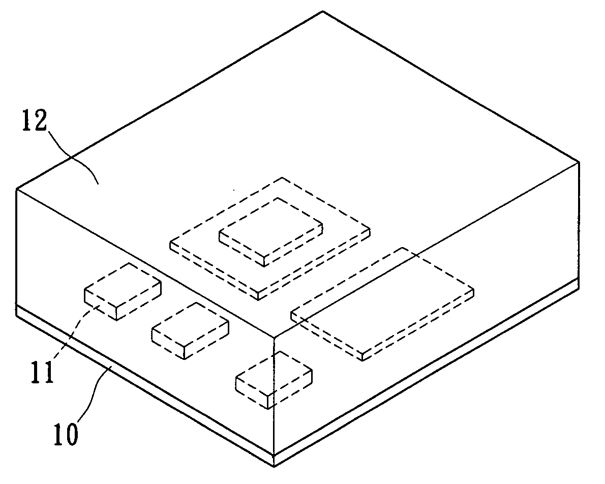
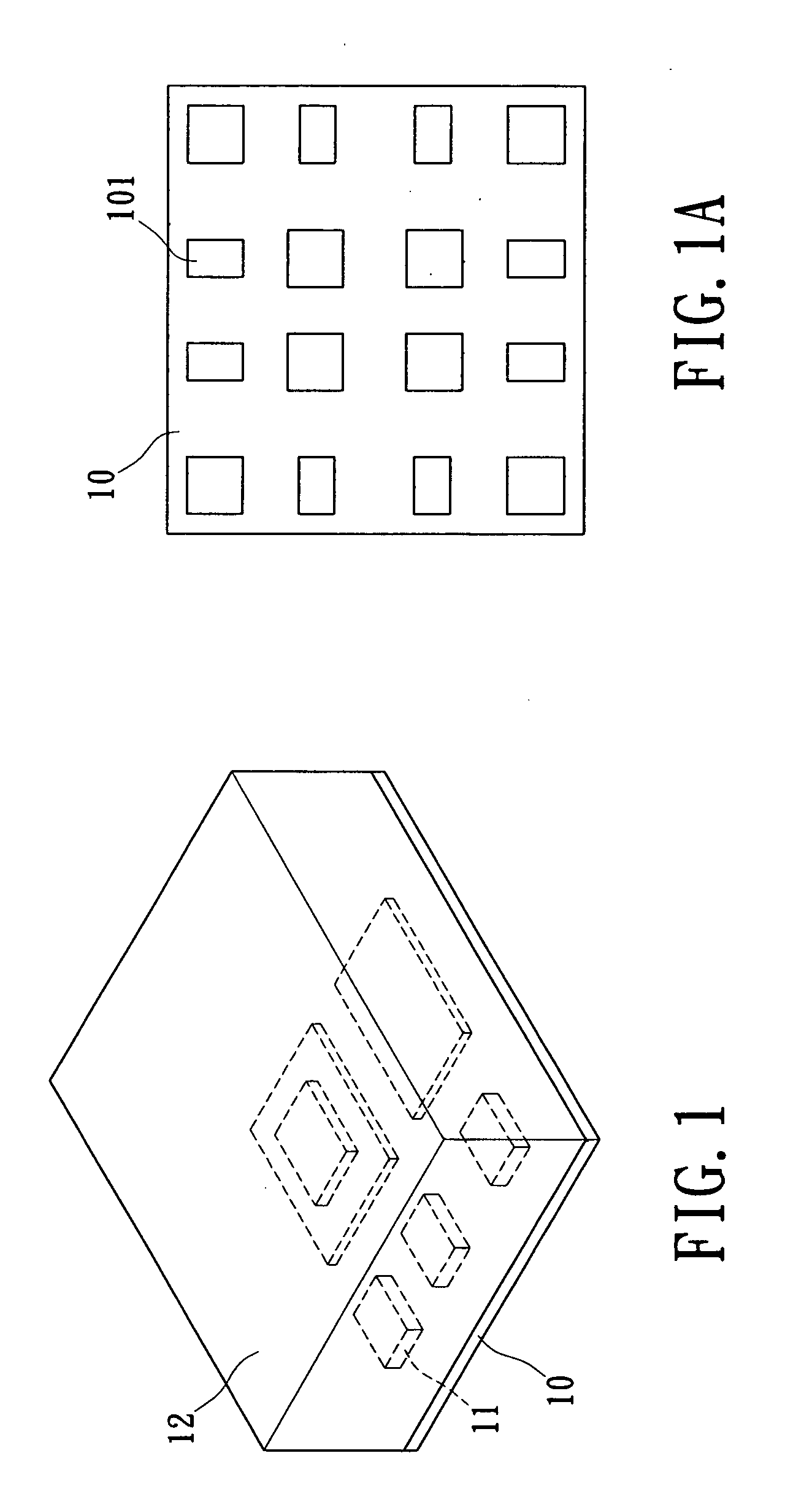
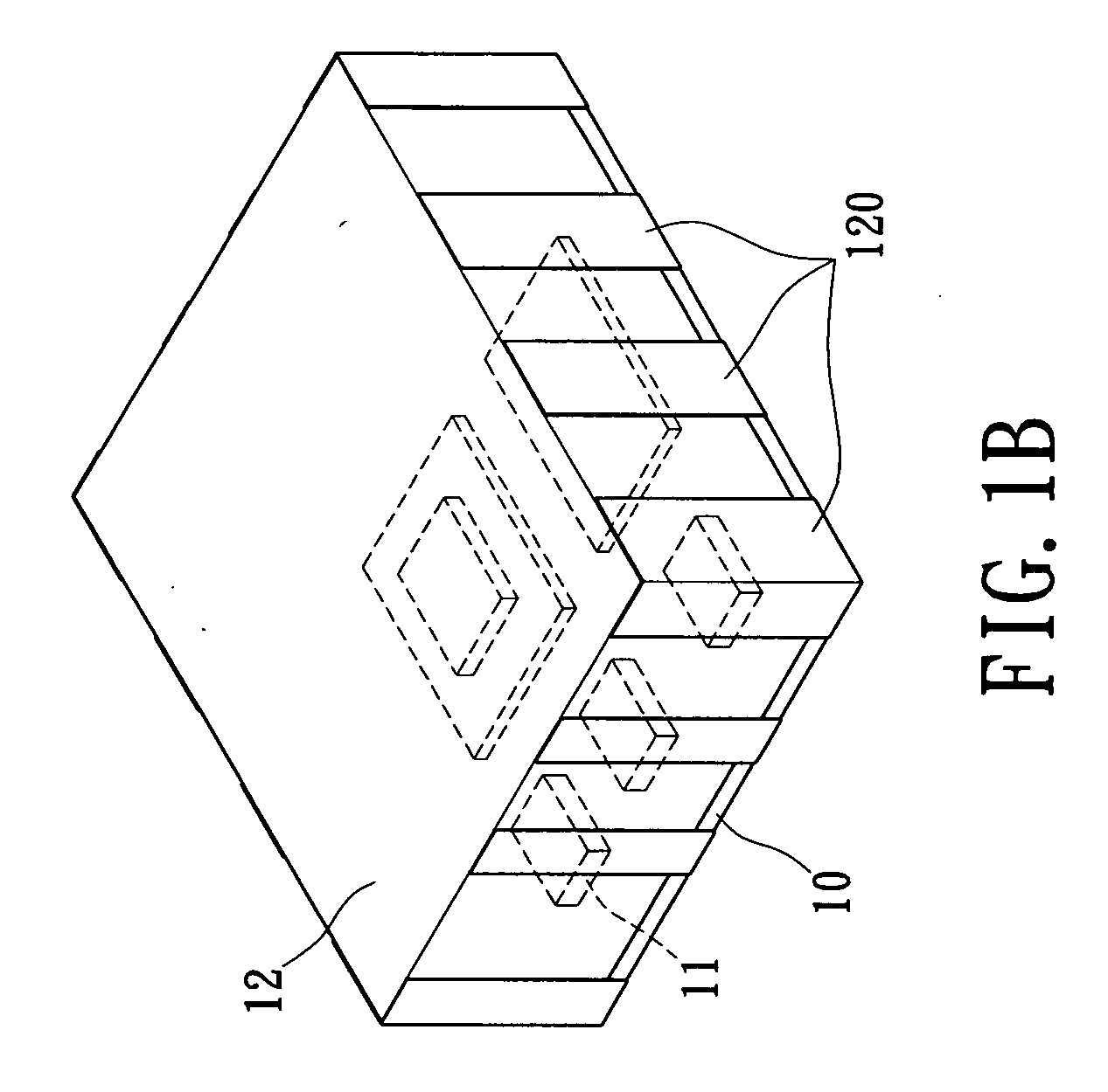
[0020]Please refer to FIG. 2; the present invention discloses an electronic packaging structure and a manufacturing method thereof. The manufacturing method is used for forming conductive lines on the sides of the module so that the modules can be stacked one on top of the other. Thus, the vertical circuit is achieved. Please refer to FIGS. 1 and 1A in conjunction to FIG. 2, the manufacturing method includes the following steps.

[0021]Step 1 is for providing an electronic module. The electronic module has a bottom surface shown in FIG. 1A, a top surface, and sides (i.e. left, right, front, and back sides) connecting between the top surface and the bottom surface. In the embodiment, the electronic module is substantially a rectangular box, but the shape of the electronic module is not restricted to this embodiment. The electronic module can be a Bluetooth module, wireless module, or another functional equivalent.

[0022]There are two methods for manufacturing the electronic module. One ...


PUM


Abstract

A packaging structure includes a main substrate having a plurality of circuit lines thereon, and an electronic module having at least one conductive pad at the bottom thereof and having a plurality of conductive lines on the sides thereof. The pad and the conductive circuits are connected electrically to the circuits on the main substrate when the electronic module is disposed on the main substrate. As above-mentioned, one electronic module can be stacked on top of another so that the integrity of the packaging structure is improved.

Description

RELATED APPLICATIONS[0001]This application is a Divisional patent application of co-pending application Ser. No. 12 / 230,531, filed on 29 Aug. 2008. The entire disclosure of the prior application, Ser. No. 12 / 230,531, from which an oath or declaration is supplied, is considered a part of the disclosure of the accompanying Divisional application and is hereby incorporated by reference.BACKGROUND OF THE INVENTION[0002]1. Field of the Invention[0003]The present invention relates to an electronic packaging structure and a manufacturing method thereof, more particularly the present invention relates to an electronic packaging structure that can be stacked with a high degree of integrity and a manufacturing method thereof.[0004]2. Description of Related Art[0005]With the development of the semiconductor technology, the function of the semiconductor chip became more and more powerful. The chip has more and more terminals to transmit the ever increasing processing data so that the packaging ...

Claims


Application Information

Patent Timeline
IPC IPC(8): H01L23/48
CPCH01L23/49805H05K1/144H05K1/187H05K3/284H05K3/3442H01L2924/0002H05K3/403H05K2203/1316H01L2924/00
Inventor HUANG, CHUNG-ERKUO, MING-TAI
Owner HUANG CHUNG ER
Why Eureka
Try Eureka