Wafer level package and method of manufacturing the same

a technology of level package and level package, which is applied in the direction of semiconductor devices, electrical equipment, semiconductor/solid-state device details, etc., can solve the problems of increasing the thickness of the entire molding resin, the need for packaging all chips for a very long time, and the increase of the process cost, so as to reduce the process cost

Inactive Publication Date: 2010-03-04
SAMSUNG ELECTRO MECHANICS CO LTD
View PDF4 Cites 17 Cited by
  • Summary
  • Abstract
  • Description
  • Claims
  • Application Information

AI Technical Summary

Benefits of technology

[0010]The present invention has been invented in order to overcome the above-described problems and it is, therefore, an object of the present invention to provide a wafer level package capable of reducing a process cost without the need for increasing a height of a metal post and allowing a metal post to play a role of a buffer to deformation of the package due to a CTE(Coefficient of Thermal Expansion) mismatch between the wafer level package and a wiring substrate by forming the metal post in a flexure hinge structure, and a method of manufacturing the same.

Problems solved by technology

A packaging process includes many unit processes, for example, chip attaching, wire bonding, molding, trimming / forming or the like, and so a conventional method of manufacturing a package to perform the packaging process by each chip has a disadvantage of needing a very long time for packaging all chips when considering the number of the chips obtained from one wafer.
In the wafer level package according to the prior art, the metal post is generally formed in a cylindrical shape and used in a state of having large compliance by increasing a height of the metal post to improve reliability, however, in this case, a thickness of the entire molding resin is increased and a process cost is rising due to increment of a plating amount in a plating process for forming the metal post.

Method used


Image

  • Wafer level package and method of manufacturing the same
  • Wafer level package and method of manufacturing the same
  • Wafer level package and method of manufacturing the same

Examples


Embodiment Construction

[0030]Hereinafter, a matter regarding to an operation effect including a technical configuration to achieve the object of a wafer level package and a method of manufacturing the same in accordance with the present invention will be appreciated clearly through the following detailed description with reference to the accompanying drawings illustrating preferable embodiments of the present invention.

[0031]A Structure of a Wafer Level Package

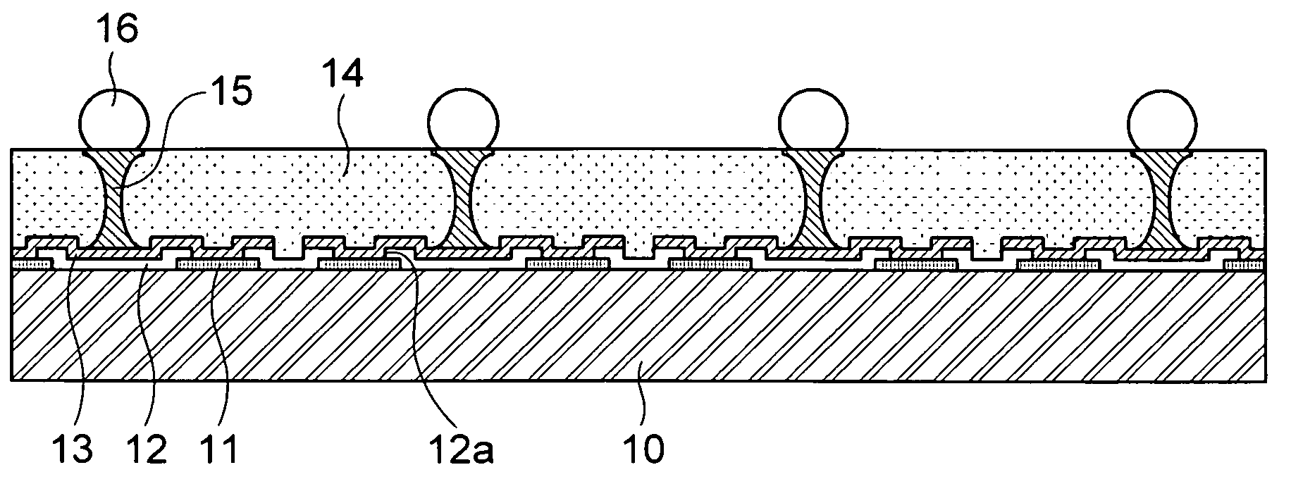
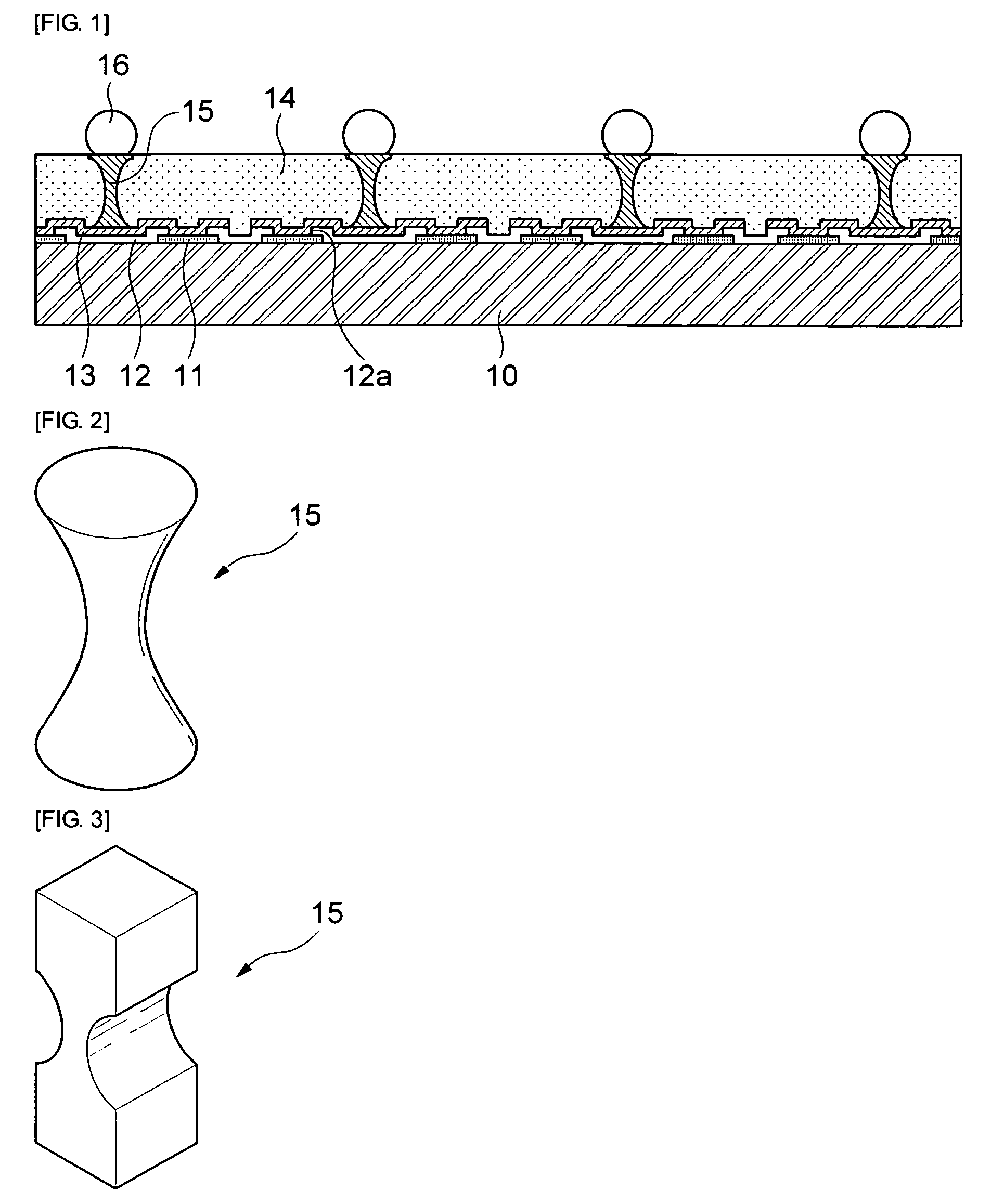
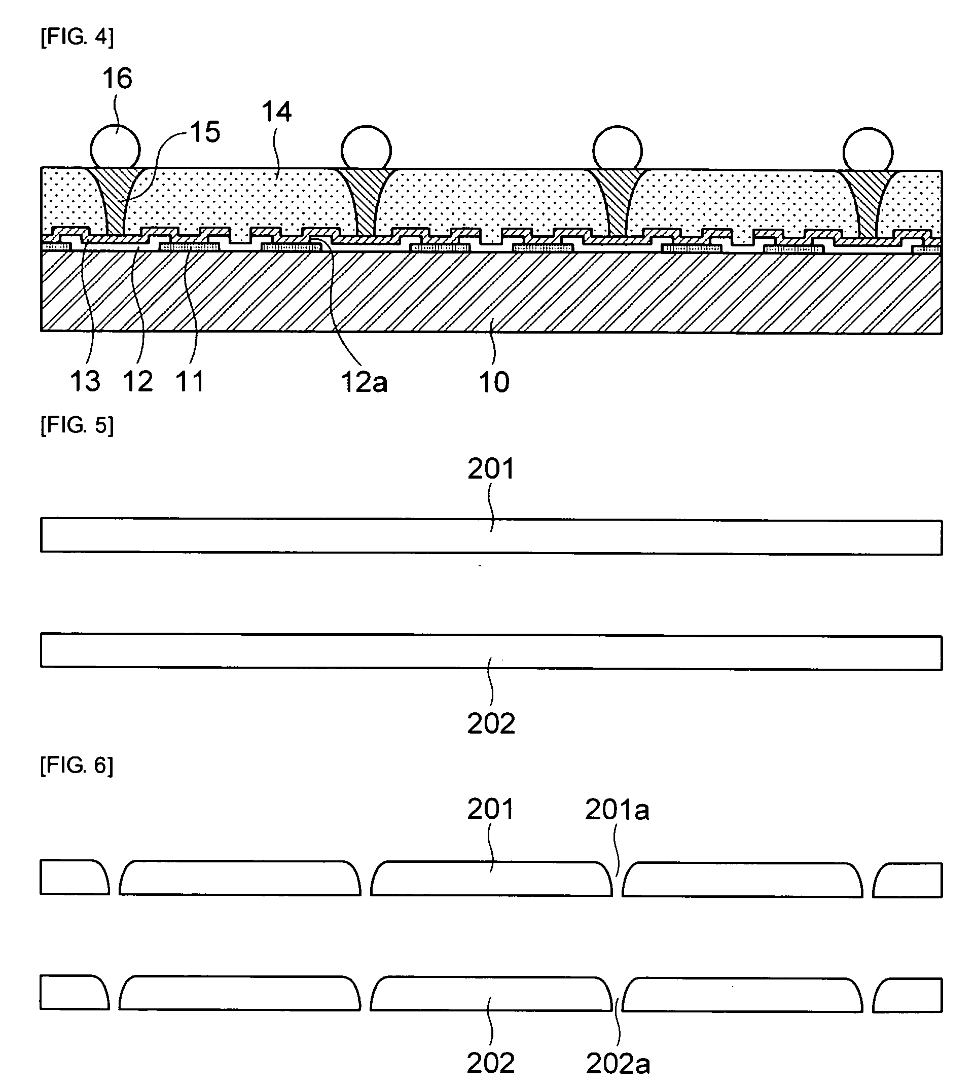
[0032]First of all, a wafer level package in accordance with an embodiment of the present invention will be described in detail with reference to FIG. 1 to FIG. 4.

[0033]FIG. 1 is a cross sectional view illustrating a structure of a wafer level package in accordance with an embodiment of the present invention, FIG. 2 and FIG. 3 are perspective views illustrating structures of metal posts in accordance with the embodiment of the present invention, FIG. 4 is a cross sectional view illustrating a structure of a wafer level package in accordance with ano...


PUM


Abstract

The present invention relates to a wafer level package and a method of manufacturing the same and provides a wafer level package structure including a wafer having a die pad; a redistribution line formed to be connected on a top surface of the die pad; a metal post connected to a top surface of the redistribution line and formed in a flexure hinge structure; and a molding resin formed between the metal posts.

Description

CROSS-REFERENCE TO RELATED APPLICATIONS[0001]This application claims the benefit of Korean Patent Application No. 10-2008-0086737 filed with the Korea Intellectual Property Office on Sep. 3, 2008, the disclosure of which is incorporated herein by reference.BACKGROUND OF THE INVENTION[0002]1. Field of the Invention[0003]The present invention relates to a wafer level package and a method of manufacturing the same; and, more particularly, to a wafer level package including a metal post with a flexure hinge structure and a method of manufacturing the same.[0004]2. Description of the Related Art[0005]A packaging process includes many unit processes, for example, chip attaching, wire bonding, molding, trimming / forming or the like, and so a conventional method of manufacturing a package to perform the packaging process by each chip has a disadvantage of needing a very long time for packaging all chips when considering the number of the chips obtained from one wafer.[0006]Therefore, recentl...

Claims


Application Information

Patent Timeline
Patent Type & Authority Applications(United States)
IPC IPC(8): H01L23/48H01L21/44
CPCH01L2924/01013H01L2224/02333H01L2924/01029H01L2924/01078H01L2924/01082H01L2924/014H01L2924/05042H01L21/76804H01L21/76817H01L21/76885H01L23/3114H01L24/02H01L24/12H01L2224/0401H01L2924/01004H01L2924/01005H01L2924/01006H01L2924/01033H01L2224/02319H01L2224/024H01L2224/0233H01L2224/0236H01L2224/0231H01L2924/01014H01L2924/181H01L2224/05557H01L2224/0348H01L2224/03472H01L24/03H01L24/05H01L24/13H01L2224/05008H01L2224/05569H01L2224/13017H01L2924/00H01L23/12H01L23/28
Inventor LEE, SEUNG SEOUPYI, SUNG
Owner SAMSUNG ELECTRO MECHANICS CO LTD
Why Eureka
Try Eureka