Inspection of underfill in integrated circuit package

a technology of integrated circuits and which is applied in the direction of gas flame welding apparatus, instruments, image data processing, etc., can solve the problems of reliability issues of ic packages, and achieve the effect of effective and efficient inspection of underfill materials

Inactive Publication Date: 2010-03-04
CHA KENG SANG +3
View PDF3 Cites 4 Cited by
  • Summary
  • Abstract
  • Description
  • Claims
  • Application Information

AI Technical Summary

Benefits of technology

[0008]Accordingly, the present invention captures a camera image that is analyzed by a data processor to effectively and efficiently inspect the underfill material dispensed in an IC package.

Problems solved by technology

Such insufficient coverage with the underfill material 112 may cause reliability issues for the IC package 100.

Method used


Image

  • Inspection of underfill in integrated circuit package
  • Inspection of underfill in integrated circuit package
  • Inspection of underfill in integrated circuit package

Examples


Embodiment Construction

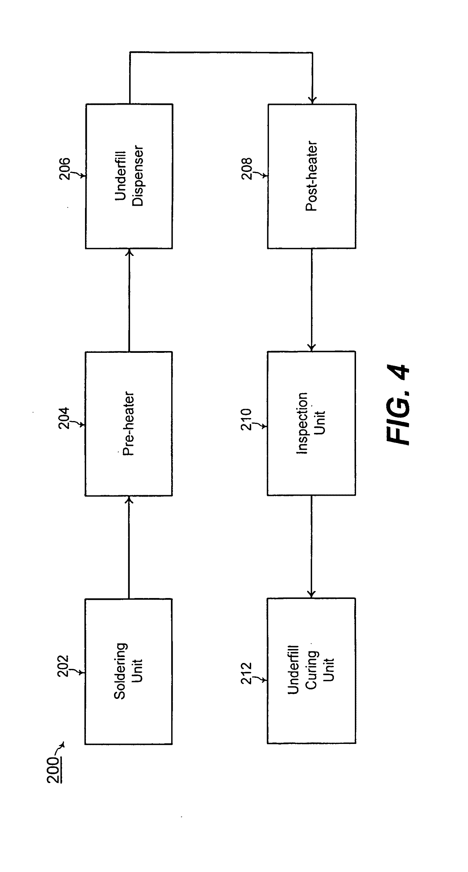
[0031]FIG. 4 shows a system 200 for properly dispensing underfill material during manufacture of an IC package. The system 200 includes a soldering unit 202, a pre-heater 204, an underfill dispenser 206, a post-heater 208, an inspection unit 210, and an underfill curing unit 212. FIG. 5 shows a flow-chart of steps during operation of the system 200 of FIG. 4.

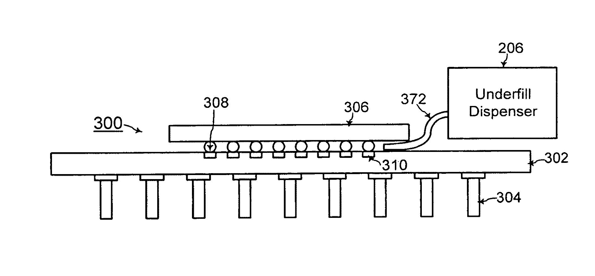
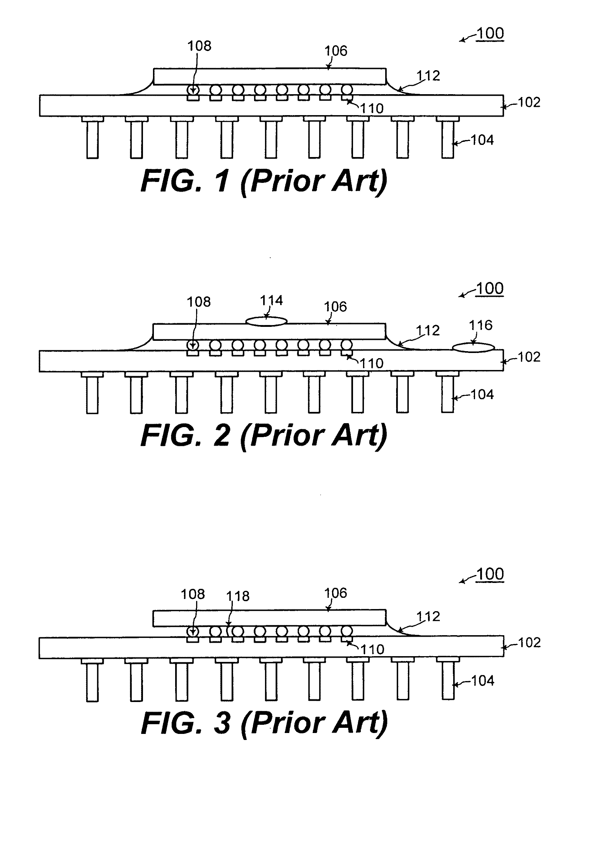
[0032]FIG. 6 shows an example IC package 300, such as a flip-chip IC package for example, processed through the system 200 of FIG. 4. The IC package 300 of FIG. 6 includes a package substrate 302 that supports pins 304 for providing electrical coupling to nodes of an integrated circuit (IC) die 306. Contact balls 308 and contact pads 310 on the substrate 302 couple such nodes of the integrated circuit die 306 to the pins 304 of the substrate 302.

[0033]The soldering unit 202 couples the contact balls 308 from the IC die 306 to the contact pads 310 of the substrate 302. For example, the contact balls 308 are soldered to the contac...


PUM

PropertyMeasurementUnit
tilted angleaaaaaaaaaa
tilt angleaaaaaaaaaa
heightaaaaaaaaaa

Abstract

In inspecting for quality of underfill material dispensed in an IC package, a camera image is captured for the IC package having the underfill material dispensed between an IC die and a package substrate. A data processor analyzes the camera image to determine an occurrence of an unacceptable condition of the underfill material. Pre-heating and / or post-heating of the package substrate before and / or after dispensing the underfill material by a contact-less heater ensures uniform spreading of the underfill material.

Description

CROSS-REFERENCE TO RELATED APPLICATION[0001]The present application is a divisional of an earlier filed copending patent application with Ser. No. 11 / 290,086 filed on Nov. 30, 2005, for which priority is claimed. This earlier filed copending patent application with Ser. No. 11 / 290,086 is in its entirety incorporated herewith by reference.TECHNICAL FIELD[0002]The present invention relates generally to integrated circuit (IC) manufacture, and more particularly, to inspection of underfill material dispensed in an IC package.BACKGROUND OF THE INVENTION[0003]FIG. 1 shows a cross-sectional view of an IC package 100, such as a flip-chip IC package for example. The IC package 100 of FIG. 1 includes a package substrate 102 that supports pins 104 for providing electrical coupling to nodes of an integrated circuit die 106. Contact balls 108 and contact pads 110 on the substrate 102 couple such nodes of the integrated circuit die 106 to the pins 104 of the substrate 102.[0004]In addition, an un...

Claims


Application Information

Patent Timeline
Patent Type & Authority Applications(United States)
IPC IPC(8): H01L21/56H01L21/66B23K3/00
CPCG06T7/0006G06T2207/30148H01L21/563H01L22/12H01L2224/73203H01L2224/16225H01L2224/73204H01L2224/32225H01L2924/00
Inventor CHA, KENG SANGTAN, TEK SENGFAZELAH, HARISSHAKIR, AHMAD ZAHRAIN B. MOHAMAD
Owner CHA KENG SANG
Why Eureka
Try Eureka