Thin-film type solar cell and method for manufacturing the same

a solar cell and thin film technology, applied in the field of thin film type solar cells, can solve the problems of not being widely used, getting more and more interest, commercialized bulk silicon solar cells not being used, etc., and achieves the effects of reducing the frequency of cutting process, simple process, and increasing the cost reduction

Inactive Publication Date: 2010-03-11
LG ELECTRONICS INC
View PDF4 Cites 23 Cited by
  • Summary
  • Abstract
  • Description
  • Claims
  • Application Information

AI Technical Summary

Benefits of technology

[0013]In the manufacturing process of a solar cell according to the related art, a portion lost by the cutting process is 100 μm or more. However, the method for manufacturing a solar cell according to the present invention reduces the frequency of the cutting process to increase the cost reducing effect in terms of manufacturing costs and provide a solar cell through simpler process. In other words, in manufacturing the thin-film type solar cell, the manufacturing method according to the related art needs to perform the cutting process numerous times. However, the present invention reduces the cutting process over the related art, as well as similar processes are simultaneously performed to unify the process to promote simplification and unification in terms of the manufacturing process, making it possible to manufacture the thin-film type solar cell with reduced manufacturing costs.
[0014]According to the present invention, the thin-film type solar cell can be manufactured at one time through a series of manufacturing processes that results in high photoelectric conversion efficiency and is relatively simple. Further, the present invention can manufacture the solar cell by reducing the frequency of patterning and the process costs.
[0015]The present invention proposes the structure and method for manufacturing the solar cell that has the high photoelectric conversion efficiency and can be manufactured at a reduced process costs. As a result, when the present invention is commercialized, the commercialized solar cell as the next-generation clean energy source contributes to the earth environment as well as may be directly applied for various fields such as public facilities, private facilities, military facilities, etc., making it possible to create a huge economic value.

Problems solved by technology

Recently, eco-friendly alternative energy is getting more and more interest due to an earth environment problem and a resource depletion problem.
Currently commercialized bulk silicon solar cells have not entered into widespread use due to high manufacturing costs and installation costs.

Method used


Image

  • Thin-film type solar cell and method for manufacturing the same
  • Thin-film type solar cell and method for manufacturing the same
  • Thin-film type solar cell and method for manufacturing the same

Examples


Embodiment Construction

[0018]Hereinafter, example embodiments of the present invention will be described in detail with reference to the accompanying drawings. In referring to reference numerals to components of each drawing, the same components are referred to by the same reference numerals as much as possible even if they are shown in different figures. Detailed descriptions of well-known techniques are omitted so as not to obscure the description of the present invention with unnecessary detail.

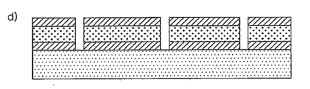
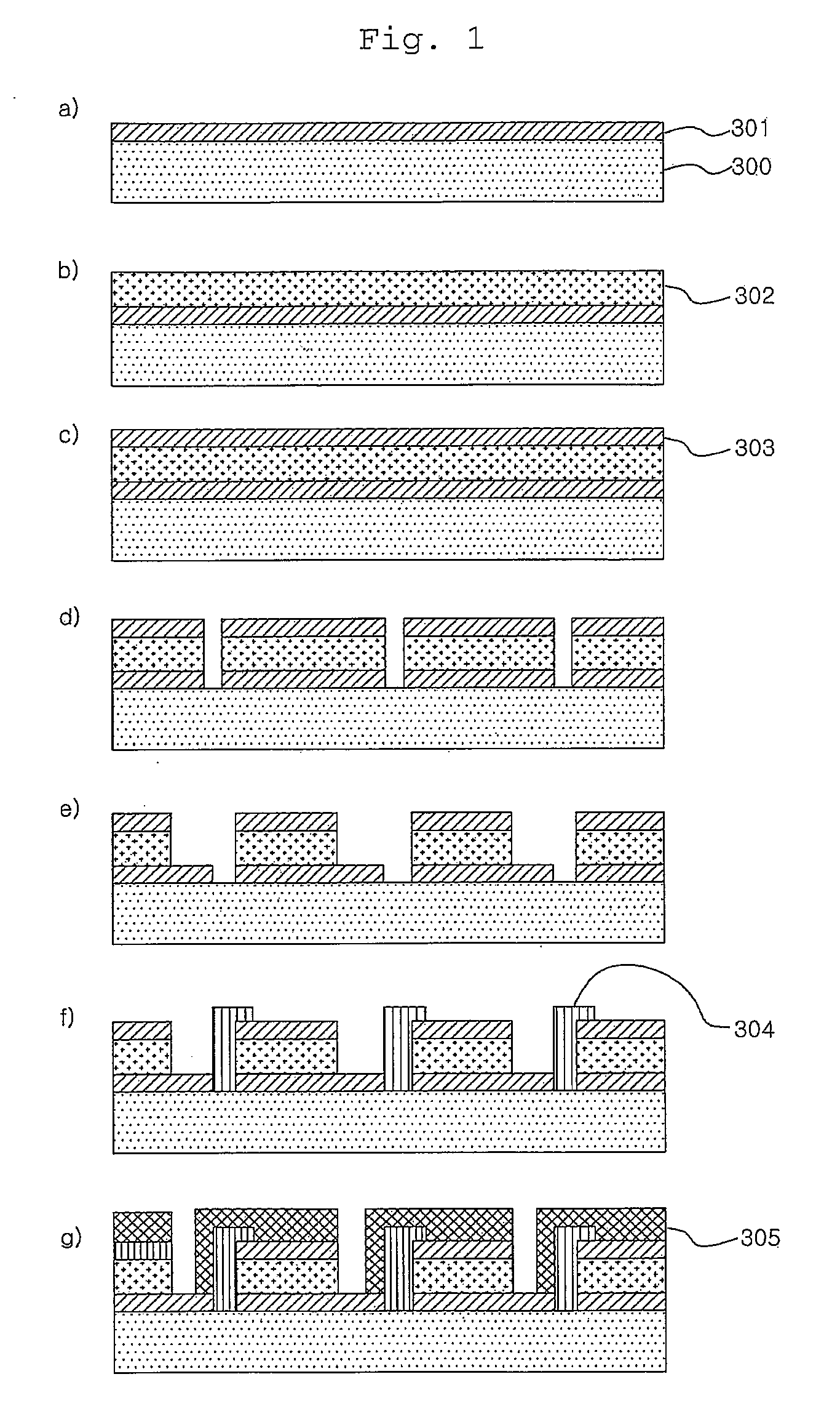
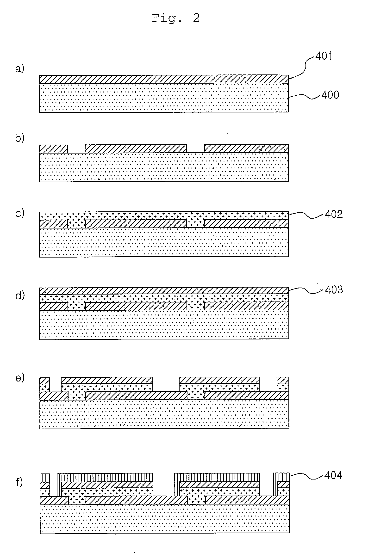
[0019]FIG. 1 is a cross-sectional view of a stacking structure of devices showing a method for manufacturing a thin-film type solar cell according to one embodiment of the present invention by each process. The following processes are only one example embodiment and may not be limited to this particular sequence.

[0020]The processes will be described in detail with reference to FIG. 1. Step (a) is an initial step for manufacturing a thin-film type solar cell of the present invention. In detail, a lower transparen...


PUM


Abstract

Disclosed are a method for manufacturing a thin-film type solar cell and a thin-film type solar cell obtained thereby that uses a direct printing method and reduces the frequency of a cutting process.

Description

BACKGROUND OF THE INVENTION[0001]This application claims priority to Korean Patent Application No. 10-2008-0085820, filed on Sep. 1, 2008, in the Korean Intellectual Property Office, the entire contents of which are hereby incorporated by reference.[0002]1. Field of the Invention[0003]The present invention relates to a thin-film type solar cell and a method for manufacturing the same, and more specifically, to a method for manufacturing a thin-film type solar cell having high photoelectric conversion efficiency while reducing process costs by reducing a frequency of a patterning process. Further, the present invention relates to a method for manufacturing a thin-film type solar cell in which a rear electrode layer is simply formed using a direct printing method in the process of sequentially forming a lower transparent electrode layer, a semiconductor layer for photoelectric conversion, and an upper transparent electrode layer on a substrate and forming each rear electrode layer aft...

Claims


Application Information

Patent Timeline
Patent Type & Authority Applications(United States)
IPC IPC(8): H01L31/042H01L31/18
CPCH01L31/0465Y02E10/50H01L31/0445H01L31/046H01L31/02167H01L31/022441H01L31/022466H01L31/02366H01L31/18
Inventor KIM, SUN HOCHOI, JUNG HOONLEE, HEON MINLEE, SEUNG-YOONEO, YOUNG JOOMOON, KANG SEOKAHN, SEH-WON
Owner LG ELECTRONICS INC
Why Eureka
Try Eureka