Bonded Wafer Assembly System and Method

a technology of bonded wafers and assemblies, applied in the field of bonded wafer assembly systems and methods, can solve the problems of increasing test time, increasing test down time, and affecting the accuracy of bonded wafers, so as to avoid the problems of alignment and cost of previous methods

Active Publication Date: 2010-03-25
TEXAS INSTR INC
View PDF16 Cites 1 Cited by
  • Summary
  • Abstract
  • Description
  • Claims
  • Application Information

AI Technical Summary

Benefits of technology

[0010]An advantage of an embodiment is that MEMS devices may be tested and further processed without singulation of the wafer. Another advantage of an embodiment is that the alignment and cost issues of associated with previous methods may be avoided.

Problems solved by technology

The use of a tape in such a process may give rise to various problems.
In particular, the shifting of chips on the tape may cause alignment problems with a testing probe or other equipment.
Such problems tend to increase test time due to extensive wafer alignment measurements, and also tend to increase the down time during testing resulting from misalignment.
Both of these factors may contribute to increased cost of semiconductor production.

Method used


Image

  • Bonded Wafer Assembly System and Method
  • Bonded Wafer Assembly System and Method
  • Bonded Wafer Assembly System and Method

Examples


Embodiment Construction

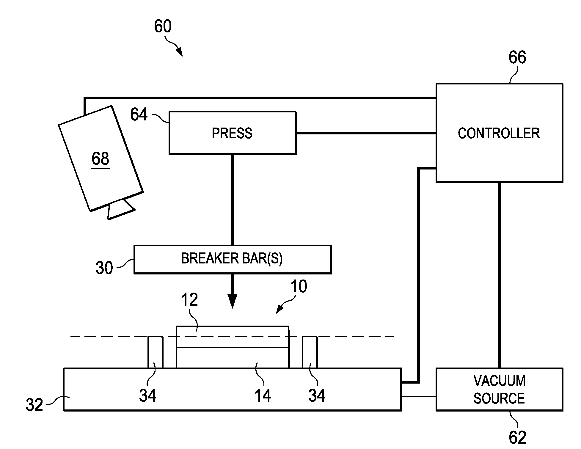
[0022]Various embodiments will now be discussed in detail with reference made to the accompanying figures. It should be appreciated, however, that the present invention provides many applicable inventive concepts that can be embodied in a wide variety of specific contexts. The specific embodiments discussed herein are merely illustrative of specific ways to make and use the invention, and do not limit the scope of the invention.

[0023]The present invention will be described with respect to preferred embodiments in a specific context, namely the fabrication of a particular microelectromechanical system (MEMS) device formed on a silicon wafer with a glass cover or cover assembly that includes a glass cover wafer, as used in, for example, a digital micromirror device (DMD). The concepts may also be applied, however, to other MEMS structures and make use of other materials as well. For example, the MEMS devices may be other spatial light modulators, other optical devices such as optical ...


PUM

PropertyMeasurementUnit
thicknessaaaaaaaaaa
widthaaaaaaaaaa
widthaaaaaaaaaa

Abstract

A system and method for the removal of superfluous material in a bonded wafer assembly. The method includes cutting a plurality of parallel cuts in a top wafer, the plurality of cuts defining a segment of the top wafer attached to another portion of the top wafer via a tab, inserting a wedge-shaped breaker bar into at least one cut of the plurality of cuts, applying force to the breaker bar to fracture the tab, and removing the segment of the top wafer from the bonded wafer assembly, wherein a bottom wafer remains unsingulated after the removing.

Description

CROSS-REFERENCE TO RELATED APPLICATIONS[0001]This application is related to co-filed and commonly owned U.S. patent application Ser. No. [Attorney Docket No. TI-66026], “MEMS Device and Fabrication Method,” which application is hereby incorporated herein by reference.TECHNICAL FIELD[0002]Embodiments of the present invention relate to a system and method for a bonded wafer assembly, and more particularly to a system and method for removing superfluous material from a MEMS bonded wafer assembly.BACKGROUND[0003]In the production of semiconductors, and particularly in the production of microelectromechanical system (MEMS) devices, chips are produced in an array often times having as many 30 or more devices on a single wafer. Typically, these devices are formed on a first wafer, and then a second wafer is bonded to the first wafer. Cavities may be formed between the wafers in various areas, for example above the MEMS components or above the bond pads. After the wafers are bonded together...

Claims


Application Information

Patent Timeline
Patent Type & Authority Applications(United States)
IPC IPC(8): H01L21/302B26F3/00B26D9/00
CPCB26F3/002B81C1/00484B81C2203/051B81C99/001B81C99/004B81C1/00888Y10T83/0341Y10T225/307Y10T225/321Y10T225/325Y10T225/329
Inventor KOEHL, DARYL ROSSD'ANDREA, BRADEN PETER
Owner TEXAS INSTR INC
Why Eureka
Try Eureka