
Inline low-damage automated failure analysis

Inactive Publication Date: 2010-04-01
GLOBALFOUNDRIES INC
View PDF18 Cites 11 Cited by
  • Summary
  • Abstract
  • Description
  • Claims
  • Application Information

AI Technical Summary

Benefits of technology

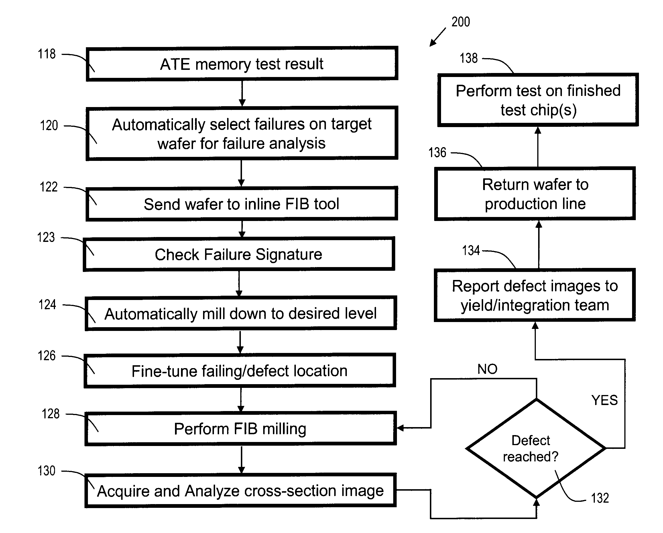
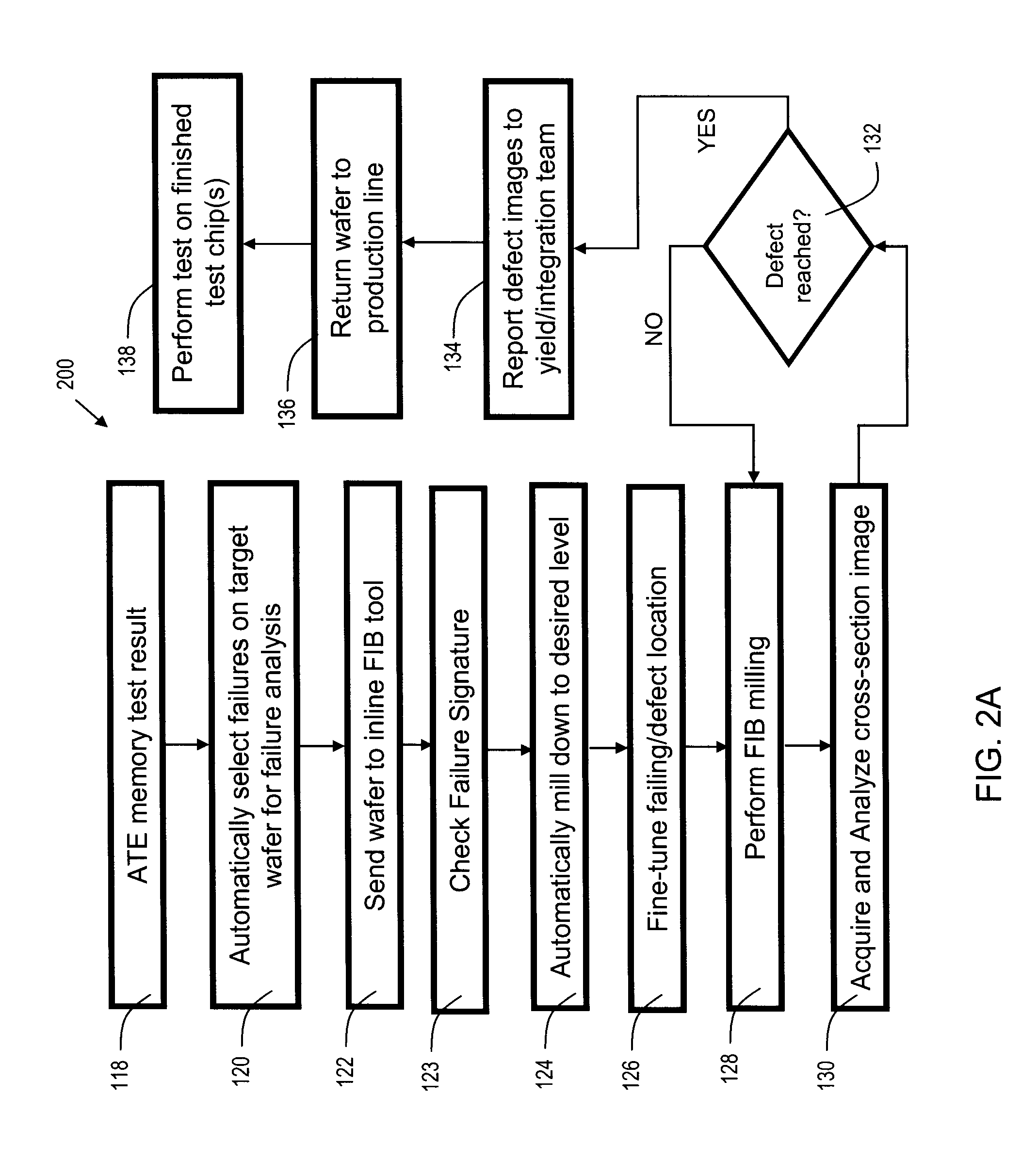
[0006]The present invention provides a method for failure analysis of devices on a semiconductor wafer, comprising the steps of: retrieving test data from an automated testing equipment tool; selecting one or more inspection points, based on failures indicated in the test data; routing the wafer to an inline focused ion beam milling tool; identifying an inspection point location by locating at least one fiducial, t

Problems solved by technology

As device geometries continue to shrink and new materials are introduced, the structural complexity of today's semiconductors grows exponentially.
Thus, the defects and structural causes of device failure are often hidden well below the surface.
Accordingly, defect analysis often requires cross-sectioning and viewing defects on a three-dimensional basis.
Furthermore, as semiconductor device densities and wafer areas increase, the volume of product diagnostic data required to diagnose yield-limiting defects grows exponentially.
This process is highly manual, and very slow.
Furthermore, the entire wafer has to be scrapped.
Since this wafer may contain many good die, scrapping the entire wafer may result in a waste of good chips.

Method used


Image

  • Inline low-damage automated failure analysis
  • Inline low-damage automated failure analysis
  • Inline low-damage automated failure analysis

Examples


Embodiment Construction

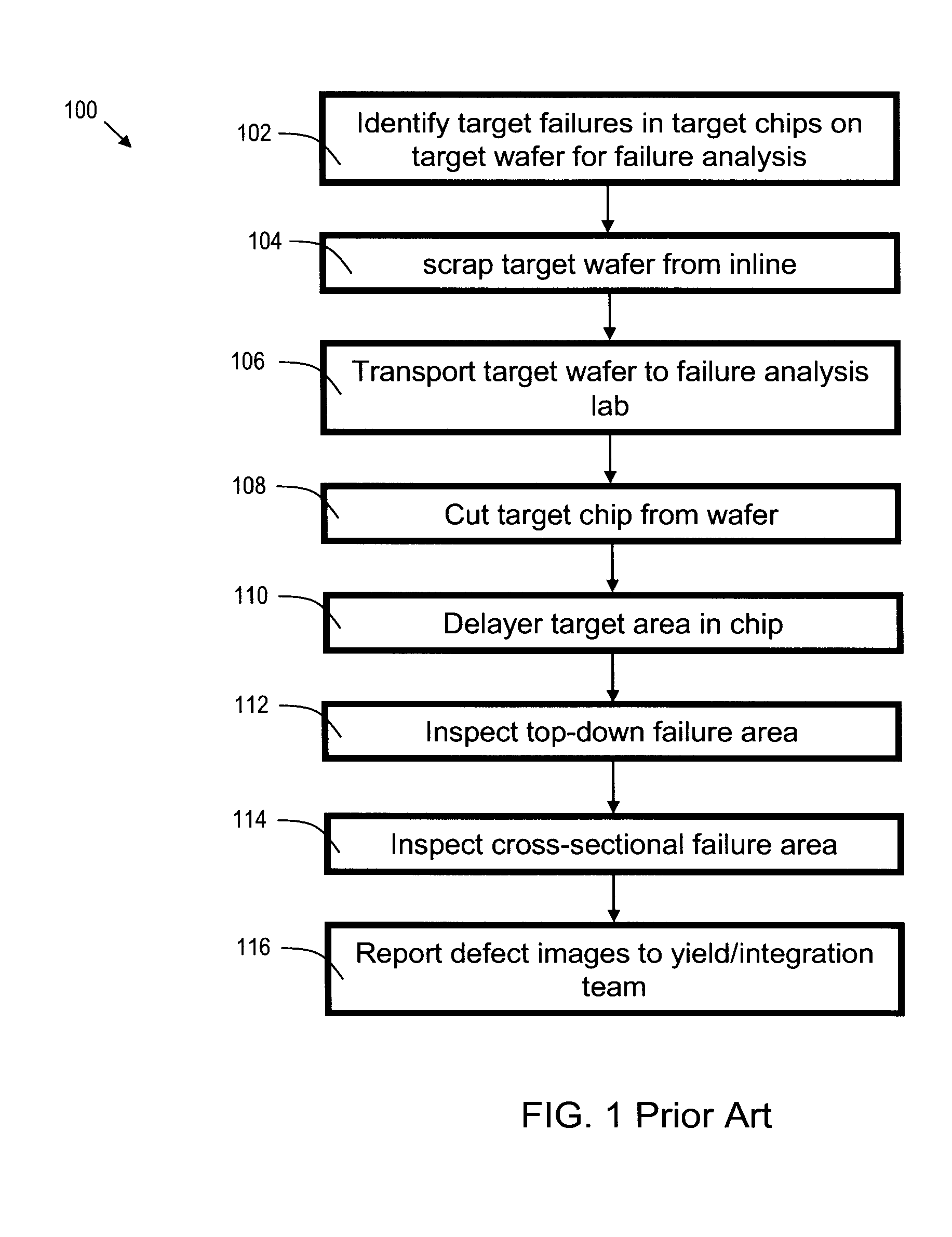
[0035]FIG. 1 is a flowchart 100 of a prior art method of failure analysis. The prior art method will be briefly reviewed here to provide context for discussion of the present invention. In process step 102, target failures are identified in one or more chips (dies) on the target wafer (the wafer to be tested). In process step 104, the target wafer is removed from inline processing, and is no longer part of the production line. In process step 106, the target wafer is transported to a failure analysis lab. This step adds considerably to the time required to perform the testing. In process step 108, the target chip (die) is removed from the wafer, again adding to the overall time required to obtain failure analysis data. In process step 110, the target area (area where the suspected failure has occurred) is delayered to the desired level, via a milling tool. In process step 112, the top-down failure area is inspected. This step can be highly manual, and hence time consuming and error ...


PUM


Abstract

A system and method for failure analysis of devices on a semiconductor wafer is disclosed. The present invention comprises the use of an inline focused ion beam milling tool to perform milling and image capturing of cross sections of a desired inspection point. The inspection points are located by identifying at least one fiducial that corresponds to an X-Y offset from the desired inspection point. The fiducials are recognized by a computer vision system. By automating the inspection process, the time required to perform the inspections is greatly reduced.

Description

FIELD OF THE INVENTION[0001]The present invention relates generally to semiconductor manufacturing. More specifically, the present invention relates to automated testing, inspection, and failure analysis of semiconductors during the manufacturing process.BACKGROUND OF THE INVENTION[0002]Engineers need to analyze defects and other failures during semiconductor fabrication to troubleshoot, adjust, and improve the fabrication processes. For example, defect analysis is useful in all aspects of semiconductor production including design verification diagnostics, production diagnostics, as well as other aspects of microcircuit research and development. As device geometries continue to shrink and new materials are introduced, the structural complexity of today's semiconductors grows exponentially. Many of the structures created are often interconnected with previous layers. Thus, the defects and structural causes of device failure are often hidden well below the surface.[0003]Accordingly, d...

Claims


Application Information

Patent Timeline
IPC IPC(8): G06K9/00G06F19/00
CPCG06T7/0004G06T2207/30148G06T2207/10061
Inventor HERSCHBEIN, STEVEN B.GEIGER, JR., RONALD C.GU, GEORGE Y.GLUSCHENKOV, OLEGOUYANG, XU
Owner GLOBALFOUNDRIES INC
Learn More