Vertical-type semiconductor device and method of manufacturing the same

Active Publication Date: 2010-04-15
SAMSUNG ELECTRONICS CO LTD
View PDF14 Cites 130 Cited by
  • Summary
  • Abstract
  • Description
  • Claims
  • Application Information

AI Technical Summary

Benefits of technology

[0009]It is therefore another feature of an embodiment to provide a vertical-type semiconductor device with a damppro

Problems solved by technology

However, formation of fine patterns may require very high-pri

Method used


Image

  • Vertical-type semiconductor device and method of manufacturing the same
  • Vertical-type semiconductor device and method of manufacturing the same
  • Vertical-type semiconductor device and method of manufacturing the same

Examples


Embodiment Construction

[0030]Korean Patent Application No. 10-2008-0098896, filed on Oct. 9, 2008, in the Korean Intellectual Property Office, and entitled: “Vertical-Type Semiconductor Device and Method of Manufacturing the Same,” is incorporated by reference herein in its entirety.

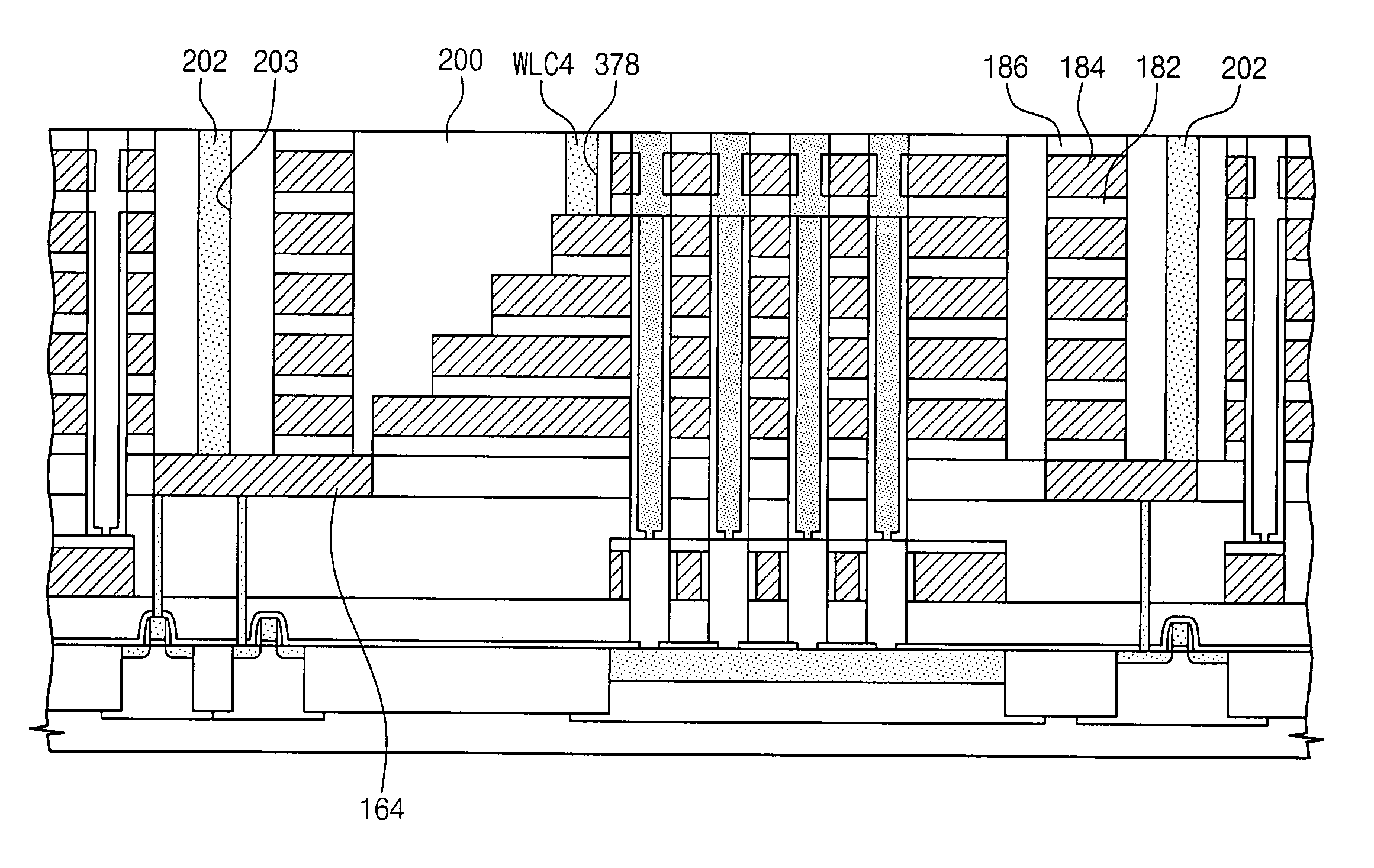
[0031]A vertical-type semiconductor device according to example embodiments may have a highly stacked structure that includes vertical semiconductor pillars through stacked wordlines. Further, the vertical-type semiconductor device according to example embodiments may include a dummy wordline structure disposed in a peripheral circuit, e.g., around the highly stacked structure, so subsequent planarization and interconnection processes of the highly stacked structure may be substantially facilitated. In other words, a high degree of difficulty of the conventional planarization and interconnection processes of the highly stacked structure may be eliminated by using the dummy wordline structure according to example embodiments.

[0...


PUM


Abstract

A vertical-type semiconductor device includes a semiconductor substrate having a cell region and a peripheral circuit region, a wordline structure on the cell region of the semiconductor substrate, the wordline structure including a plurality of wordlines stacked on top of each other, a semiconductor structure through the wordline structure, a gate dielectric between the wordline structure and the semiconductor structure, and a dummy wordline structure on the peripheral circuit region, the dummy wordline structure having a vertical structure and including same components as the wordline structure.

Description

BACKGROUND[0001]1. Field[0002]Example embodiments relate to a semiconductor device and a method of manufacturing the same. More particularly, example embodiments relate to a vertical-type semiconductor device and a method of manufacturing the same.[0003]2. Description of the Related Art[0004]In order to satisfy superior performance and inexpensive prices in semiconductor devices, an increased degree of integration of semiconductor devices may be required. In case of memory semiconductor devices, since a degree of integration is a key factor determining a price of a product, highly integrated semiconductor devices may be required.[0005]In case of typical two-dimensional or planar memory semiconductor devices, since a degree of integration thereof is related to an area occupied by a unit memory cell, integration may be affected by fine pattern formation technologies. However, formation of fine patterns may require very high-priced devices, thereby limiting a degree of integration ther...

Claims


Application Information

Patent Timeline
IPC IPC(8): H01L27/105H01L21/8239
CPCH01L27/11526H01L27/11529H01L27/11551H01L27/11556H01L27/11573H01L29/7926H01L29/66825H01L29/66833H01L29/7881H01L29/792H01L27/11578H10B41/40H10B41/41H10B41/20H10B43/40H10B43/20H10B41/27
Inventor LEE, SEUNG-JUNLEE, WOONKYUNG
Owner SAMSUNG ELECTRONICS CO LTD
Why Eureka
Try Eureka