Test system for flicker noise

a test system and flicker noise technology, applied in the direction of noise figure or signal-to-noise ratio measurement, measurement device, instruments, etc., can solve the problem of shooting noise, the noise level of the device itself or a combination of devices, and the signal-to-noise ratio decreas

Active Publication Date: 2010-05-27
FORMFACTOR INC
View PDF103 Cites 16 Cited by
  • Summary
  • Abstract
  • Description
  • Claims
  • Application Information

AI Technical Summary

Problems solved by technology

One of the performance characteristics of interest for an electrical device is the noise level of the device itself or a combination of devices.
However, the device itself may produce additional noise, that when added to the input noise, results in a decrease in the signal-to-noise ratio.
Shot noise is typically generated where there is a potential barrier (voltage differential).
Shot noise is generated when the electrons and holes cross the barrier.
However, current flowing through a diode and similar devices produces small signal fluctuations.
Flicker noise is associated with crystal surface defects in semiconductors.
Flicker noise tends to be essentially random in nature, but, because its frequency spectrum is not flat, it is not considered a true white noise.
Flicker noise becomes more pronounced with smaller device geometries and lower operating voltages.
For higher frequency, lower voltage digital circuits with higher data rates flicker noise is a dominant cause of logic errors increasing the importance of accurate measurements of flicker noise.
Flicker noise increases as the size of devices decreases and as the flicker noise increases so does the flicker noise bandwidth.

Method used


Image

  • Test system for flicker noise
  • Test system for flicker noise
  • Test system for flicker noise

Examples


Embodiment Construction

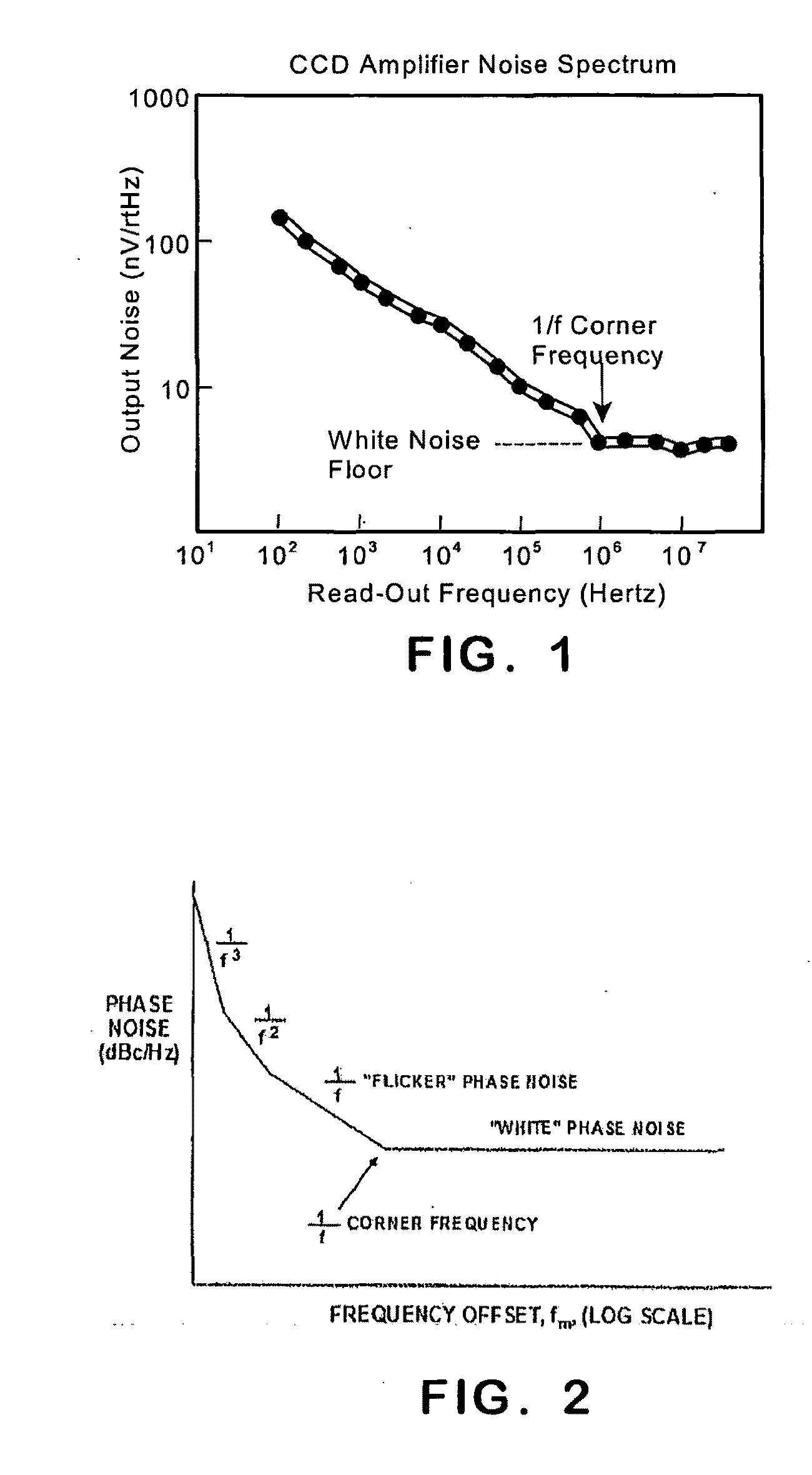
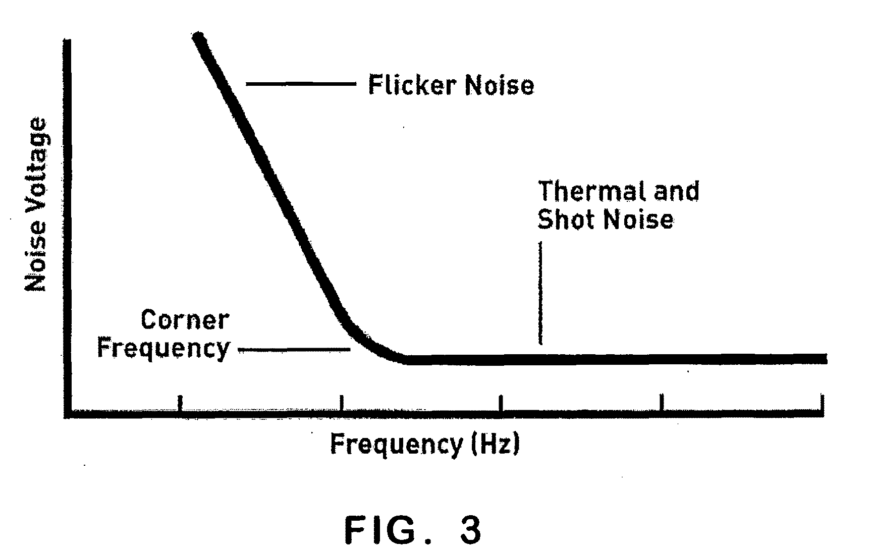
[0037]Flicker noise increases as the size of a device decreases and an increase in flicker noise increases the flicker noise bandwidth, the measurement range required to fully characterize the flicker noise. Characterizing the flicker noise of smaller devices requires measurement system components with a good frequency response, elimination or control of electrical noise that might affect the system and accurate DC measurements for the device under test.

[0038]Integrated circuits (ICs) include micro-circuits chemically etched on and into semiconductor material or wafers. It is customary to manufacture several ICs on a single wafer and then separate the individual circuits after performance and functional testing in a wafer probe station. The test points on ICs are customarily laid out along rectangular grid coordinates and may be tested with multiple probes on a probe card or by single probes in a north-south-east-west arrangement. Likewise, ICs in a composite device are typically ar...


PUM


Abstract

A flicker noise test system includes a guarded signal path and an unguarded signal path selectively connectable to respective terminals of a device under test. The selected signal path is connectable a terminal without disconnecting cables or changing probes.

Description

CROSS-REFERENCE TO RELATED APPLICATIONS[0001]This application claims the benefit of U.S. Provisional Application No. 61 / 200,187, filed Nov. 24, 2008.BACKGROUND OF THE INVENTION[0002]The present invention is directed to probe equipment for low noise measurements.[0003]It is sometimes desirable to determine the functional characteristics and / or the performance of an electrical device, such as an integrated circuit. One of the performance characteristics of interest for an electrical device is the noise level of the device itself or a combination of devices. The noise contribution of each device in a signal path should be sufficiently low that collectively they do not interfere with the ability to detect the signals. Typically, the level of the noise is referred to as the signal to noise ratio of the device. In some cases, the level of the noise is relative to a known potential, such as ground.[0004]The level of the noise of a device, such as the noise observed at the collector or drai...

Claims


Application Information

Patent Timeline
Patent Type & Authority Applications(United States)
IPC IPC(8): G01R29/26
CPCG01R29/26G01R1/18
Inventor NEGISHI, KAZUKIHANSEN, MARK
Owner FORMFACTOR INC
Why Eureka
Try Eureka